ALLPCB


Overview
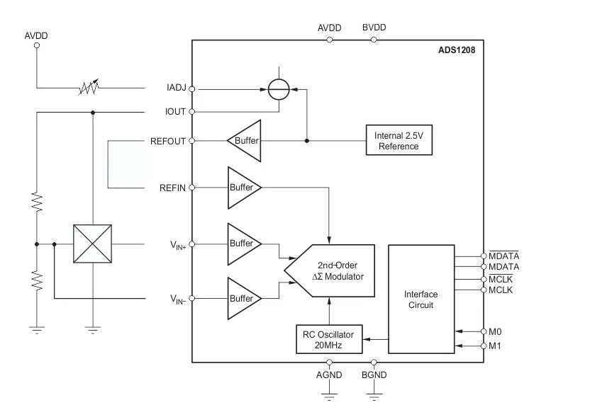
Demand for high-precision, high-performance analog-to-digital conversion is increasing in electronic design. Texas Instruments' ADS1208 is a second-order delta-sigma modulator optimized for Hall sensors and similar applications. It operates with a nominal clock frequency of 10 MHz, offers a specified input range of ±100 mV and a full-scale range of ±125 mV, a typical common-mode rejection (CMR) of 95 dB, and a typical signal-to-noise ratio (SNR) of 82 dB. The device includes a programmable current output for sensor biasing, digital outputs compatible with the ADS1202/03, differential digital outputs, and an independent 2.7 V to 5.5 V digital supply pin.
Key Features
High-precision measurements
- Resolution and linearity: The ADS1208 provides 16-bit resolution. Integral nonlinearity (INL) at 16-bit resolution is -8 to 8 LSB (or -0.012% to 0.012%), and differential nonlinearity (DNL) is -1.0 to 1.0 LSB, enabling high-precision measurements.
- Low-noise performance: Low-noise analog inputs and strong common-mode rejection reduce external interference and help ensure measurement accuracy.
Flexible configuration
- Programmable current source: An internal programmable current source can bias sensors. The output current is programmed by placing a resistor between AVDD and IADJ, with a range of 1 mA to 8 mA.
- Multiple operating modes: Four operating modes are supported, allowing selection of clock source and data output method to match application requirements.
Compatibility
Digital outputs are compatible with the ADS1202/03, facilitating integration and substitution across different projects.
Applications
Motor control
Accurate current measurement is critical in motor control. The ADS1208's high precision and low noise enable accurate motor current sensing to support precise control.
Current measurement
Suitable for both large current measurements in industrial contexts and low-current monitoring in electronic devices, the ADS1208's input range and precision ensure accurate measurements.
Sensor interfaces
Designed for Hall sensors and bridge sensors, the device provides stable bias current and converts sensor analog signals into digital streams for downstream processing.
Technical Details
Analog section
- Modulator: The second-order modulator acts as a filter that low-pass filters the input while pushing quantization noise to higher frequencies. A digital low-pass filter is required at the output to remove high-frequency noise and to convert the 1-bit data stream into multi-bit words.
- Analog input: Internal sampling capacitors must recharge within 50 ns. The ADS1208 provides two input buffers with high bandwidth (typical 50 MHz), low noise, and low offset, which improves system performance, especially with higher source impedances.
- Internal reference: A 2.5 V reference is provided, with output tolerance from 2.45 V to 2.55 V and temperature drift of 20 ppm/°C. The REFIN pin accepts an external reference from 0.5 V to 3 V to set the analog input range.
- Current source: The integrated current source can bias Hall elements. The output current is set by the resistor R_ADJ. Under certain conditions, reference drift can be compensated, and adjusting the resistor can calibrate system gain.
Digital section
- Digital output behavior: There is a defined relationship between differential analog input and the output bitstream. For example, 0 V input corresponds to 50% high time, +100 mV corresponds to 80% high time, and -100 mV corresponds to 20% high time.
- Digital interface: Four operating modes are supported, with different clock sources and data output schemes per mode. The internal clock can be derived from a 20 MHz RC oscillator or from an external clock. The digital I/O voltage range is 2.7 V to 5.5 V for broad compatibility.
- Filter selection: The modulator bitstream requires digital filtering to produce a digital word proportional to the analog input. A Sinc3 filter is simple and effective for many applications. For applications requiring faster response, such as motor control, other filters like Sinc2 may be preferable.
Layout Considerations
Power supply
The ADS1208 uses an analog supply (AVDD) and a digital supply (BVDD). The analog supply must be stable and low-noise to ensure measurement accuracy. Placing a 5 Ω resistor between supplies and using decoupling capacitors for filtering is recommended. Avoid applying input signals before power-up to prevent latch-up.
Grounding
Separate analog and digital ground planes and connect them under the modulator with short signal traces. For multiple modulators, connect the grounds at a single central point when possible.
Decoupling
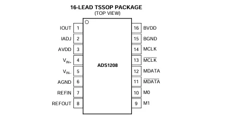
Place decoupling capacitors as close to their respective pins as possible. For the 100 nF bypass between AVDD and AGND, placing the capacitor directly at pins 3 and 6 reduces internal current spikes' effect on the supply and improves noise performance.
Summary
The ADS1208 second-order delta-sigma modulator offers high precision, configurability, and compatibility for motor control, current sensing, and sensor interface applications. Understanding its electrical characteristics, operating modes, filter options, and PCB layout requirements helps achieve optimal system performance.