If you're new to the world of printed circuit boards (PCBs), you might be wondering, what is PCB imaging? Simply put, PCB imaging is a critical step in the PCB manufacturing process where a design pattern is transferred onto a substrate to create the conductive pathways for electronic components. This guide will dive deep into the PCB imaging process, explore various PCB imaging methods, highlight essential PCB imaging equipment, and provide a clear roadmap for PCB imaging for beginners. Whether you're a hobbyist or an aspiring engineer, this blog will break down the basics to help you understand this foundational aspect of PCB production.
What Is PCB Imaging? A Simple Explanation
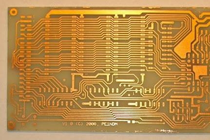
PCB imaging is the process of transferring a circuit design onto a board material, typically a copper-clad laminate, to define where the conductive tracks, pads, and other features will be. Think of it as creating a blueprint on the board that tells manufacturers where to place copper and where to remove it. This step is crucial because it directly impacts the accuracy and functionality of the final PCB.
In essence, PCB imaging sets the stage for etching, where unwanted copper is removed to reveal the circuit pattern. Without precise imaging, the board's electrical connections could fail, leading to a malfunctioning device. For beginners, understanding this process is the first step toward mastering PCB design and fabrication.
Why Is PCB Imaging Important?
The importance of PCB imaging lies in its role as the foundation of PCB manufacturing. A small error during imaging can lead to misaligned traces, short circuits, or open connections, rendering the board useless. For example, if a trace is off by just 0.1 mm, it could cause signal integrity issues, especially in high-speed circuits where impedance matching is critical (typically around 50 ohms for many applications).
Accurate imaging ensures that the PCB meets the design specifications, supports the intended electrical performance, and fits within the mechanical constraints of the device. For beginners, mastering the basics of imaging can save time, reduce costs, and prevent frustration during prototyping.
The PCB Imaging Process: Step-by-Step for Beginners
The PCB imaging process can seem complex at first, but breaking it down into steps makes it easier to grasp. Here's a beginner-friendly overview of how it works:
1. Design Preparation
Before imaging begins, the PCB design is created using specialized software. This design includes the layout of traces, pads, vias, and other features. The design is then exported as a set of files (often in Gerber format) that represent each layer of the PCB. These files act as the "instructions" for the imaging process.
2. Cleaning the Substrate
The copper-clad board, which serves as the base material, is thoroughly cleaned to remove dirt, oil, or oxidation. A clean surface is essential for proper adhesion of the imaging material, ensuring the pattern transfers accurately.
3. Applying Photoresist
A light-sensitive material called photoresist is applied to the copper surface. This can be done as a liquid coating or a dry film. The photoresist will either harden or remain soluble when exposed to light, depending on whether it's positive or negative photoresist.
4. Exposing the Pattern
The board is placed under a light source, and the design pattern (from the Gerber files) is projected onto the photoresist using a photomask or direct imaging technology. Areas exposed to light (or unexposed, depending on the photoresist type) will define the circuit pattern.
5. Developing the Image
After exposure, the board is immersed in a developer solution. This removes the unhardened photoresist, leaving behind the desired circuit pattern on the copper. At this stage, the copper is still intact, but the pattern is now visible as protected areas of photoresist.
6. Inspection
The board is inspected for defects, such as incomplete patterns or misalignments. For beginners, this step is critical to catch errors before moving to etching, where mistakes become permanent.
Common PCB Imaging Methods: Which One to Choose?
There are several PCB imaging methods used in the industry, each with its own advantages and suited for different levels of complexity. As a beginner, understanding these methods will help you choose the right approach for your project.
1. Photolithography with Photomasks
This traditional method uses a physical photomask—a transparent film with the circuit pattern printed on it—to expose the photoresist. It's widely used for its reliability and is ideal for small to medium production runs. However, creating photomasks can be time-consuming and costly for one-off prototypes.
2. Direct Digital Imaging (DDI)
Direct Digital Imaging skips the photomask and uses a laser or LED to directly project the design onto the photoresist. This method is faster and more flexible, making it perfect for prototyping and small batches. It also reduces costs since there's no need for a physical mask.
3. Inkjet Printing for Imaging
An emerging method, inkjet printing, deposits a light-blocking material directly onto the board to create the pattern. While not as common for professional PCBs, it's an accessible option for hobbyists experimenting with DIY imaging at home.
For beginners, starting with Direct Digital Imaging can be a practical choice due to its flexibility and lower upfront costs. As you gain experience, exploring photolithography can provide insight into industrial processes.
Essential PCB Imaging Equipment for Beginners
Getting started with PCB imaging equipment doesn't have to be overwhelming. While industrial setups use advanced machinery, beginners can work with more affordable tools to learn the basics. Here's a rundown of the essential equipment:
1. UV Exposure Unit
A UV exposure unit is used to expose the photoresist on the board. For hobbyists, a simple UV light box (priced between $50-$150) can work for small projects. These units typically use UV bulbs with a wavelength of 365 nm, ideal for most photoresists.
2. Photoresist Materials
You'll need either liquid photoresist or dry film photoresist. Dry film is easier for beginners to handle and costs around $10-$20 for a small roll, enough for several boards. Ensure the photoresist matches your exposure unit's wavelength.
3. Developer Solution
A developer chemical removes unexposed photoresist after exposure. Sodium carbonate solutions are common and cost about $5-$10 for a small quantity. Always handle chemicals with care and follow safety guidelines.
4. Transparency Film or Printer (for Photomasks)
If using the photomask method, you'll need transparency film and a high-resolution printer (at least 1200 DPI) to print your design. A decent printer can cost $100-$300, but it's a one-time investment for multiple projects.
5. Cleaning Supplies
Basic supplies like isopropyl alcohol, scrub pads, and gloves (total cost under $20) are necessary to clean the board before imaging. Cleanliness prevents defects in the pattern transfer.
For beginners on a budget, start with a basic UV exposure unit and dry film photoresist. As you progress, investing in a small laser engraver for Direct Digital Imaging (around $300-$500) can streamline the process.
Tips for Successful PCB Imaging for Beginners
Starting with PCB imaging for beginners can be challenging, but these practical tips will help you achieve better results and avoid common pitfalls:
- Double-Check Your Design: Before imaging, ensure your design files are error-free. Misaligned layers or incorrect trace widths (e.g., below 0.2 mm for most processes) can cause failures.
- Control Exposure Time: Overexposure or underexposure can ruin the photoresist pattern. Test with small exposure increments (e.g., 30-second intervals) to find the optimal time, typically 2-5 minutes for most UV units.
- Maintain a Clean Workspace: Dust or fingerprints on the board can create defects. Work in a clean, well-ventilated area and wear gloves when handling materials.
- Use Proper Safety Gear: When working with chemicals like developers, wear protective gloves and goggles to avoid skin or eye irritation.
- Start Small: Begin with simple designs (e.g., single-layer boards with traces wider than 0.3 mm) to build confidence before tackling complex multilayer projects.
Common Challenges in PCB Imaging and How to Overcome Them
As a beginner, you might face a few hurdles during PCB imaging. Here are some common issues and solutions:
1. Incomplete Pattern Transfer
If parts of the pattern don't transfer properly, it could be due to underexposure or uneven photoresist application. Check your exposure time and ensure the photoresist is applied uniformly. For dry film, use a laminator for even adhesion.
2. Misaligned Layers
Misalignment often happens when manually aligning photomasks or boards. Use alignment marks in your design and secure the board during exposure to prevent movement.
3. Defects in Photoresist
Bubbles or wrinkles in the photoresist can distort the pattern. Apply the film slowly and smooth out any imperfections before exposure. For liquid photoresist, ensure even coating with a roller or brush.
How PCB Imaging Fits Into the Larger Manufacturing Process
PCB imaging is just one part of the broader PCB manufacturing journey. After imaging, the board undergoes etching to remove unwanted copper, followed by drilling for vias and holes, plating to strengthen connections, and applying solder mask and silkscreen for protection and labeling. Each step builds on the accuracy of the imaging process, highlighting its importance.
For beginners, focusing on imaging helps build a strong foundation. Once you're comfortable with creating accurate patterns, you can explore other stages like etching (often using ferric chloride, which removes copper at a rate of about 0.025 mm per minute) and assembly.
Conclusion: Start Your PCB Imaging Journey Today
Understanding the basics of PCB imaging is a vital step for anyone entering the world of electronics design and manufacturing. From grasping what is PCB imaging to exploring the PCB imaging process, methods, and equipment, this guide has equipped you with the knowledge to get started. With the right tools and a bit of practice, PCB imaging for beginners becomes an achievable skill that opens the door to creating custom circuit boards for your projects.
Remember to start small, prioritize cleanliness and precision, and don't hesitate to experiment with different imaging techniques. As you gain experience, you'll refine your process and tackle more complex designs with confidence. Dive into PCB imaging today, and watch your electronic ideas come to life!
 ALLPCB


