ALLPCB


Diodes are among the most common components on circuit boards. What factors should be considered when selecting them?
1. Forward conduction voltage (VF)
Voltage drop: the potential change across a component when current flows through it, relative to a common reference point, often abbreviated as voltage drop.
Forward conduction voltage: the voltage at which the diode begins to conduct.
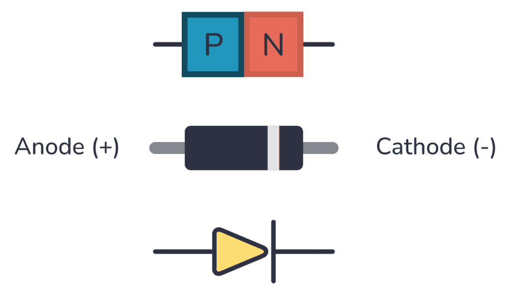
Forward characteristic: when a forward voltage is applied to a diode, at the initial region the forward voltage is too small to overcome the PN junction electric field, so forward current is nearly zero. As forward voltage increases enough to overcome the junction field, the diode conducts and current rises rapidly with voltage.
2. Rated current and maximum forward current (IF)
The rated current IF is the average current value calculated from the allowable operating temperature rise for long-term operation. Current high-power rectifier diodes can have IF values up to 1000 A.
It denotes the maximum allowable continuous forward average current for long-term operation and depends on PN junction area and external cooling conditions. Current flow heats the device; if temperature rises beyond allowable limits (approximately 141 for silicon devices and 90 for germanium devices), the die can overheat and be damaged.
3. Maximum average rectified current (Io)
Maximum average rectified current IO: in a half-wave rectifier circuit, the maximum value of the average rectified current flowing through the load resistor. This is an important value for design calculations.
4. Maximum surge current (IFSM)
Surge current denotes excess instantaneous forward current that flows during operation. It is not a normal operating current but a large transient current.
5. Maximum repetitive peak reverse voltage (VRM)
Even without reverse current, continuously increasing the reverse voltage will eventually damage the diode. For devices exposed to alternating voltages, the maximum repetitive peak reverse voltage VRM is the maximum repeatedly applied reverse peak voltage to avoid breakdown. VRM ratings can reach several kilovolts.
6. Maximum reverse voltage (VR)
The maximum reverse peak from repeated AC is VRM; VR refers to the value of a continuously applied DC reverse voltage. The maximum DC reverse voltage is important for determining allowable limits in DC applications.
Related Reading: TVS Diode Characteristics & Parameters
7. Maximum operating frequency (fM)
Because of the junction capacitance of the PN junction, a diode's unidirectional conduction deteriorates above a certain frequency. Point-contact diodes have high fM values (above 100 MHz); rectifier diodes have lower fM values, typically no higher than a few kHz.
8. Reverse recovery time (Trr)
When the applied voltage switches from forward to reverse, ideally the diode current would stop instantly. In practice there is a short delay. The reverse recovery time quantifies the delay before the current ceases.
9. Maximum power (P)
When current flows through a diode it dissipates heat, raising its temperature. Maximum power P is the maximum allowable power dissipation, calculated as the voltage across the diode multiplied by the current through it. This parameter is especially important for Zener diodes and variable-resistance diodes.
10. Reverse saturation leakage current (IR)
The current flowing when a reverse voltage is applied across a diode, dependent on semiconductor material and temperature. At room temperature, silicon diodes have IR in the nA (10^-9 A) range, while germanium diodes are in the μA to mA range (around 10^-6 A).
Related Reading: The Engineer's Guide to Selecting the Right Diode for Reverse Polarity Protection
11. Derating (junction temperature derating)
Derating improves product reliability and extends service life. According to the rule of thumb that reducing temperature by 10°C doubles lifetime, the table below lists minimum derated junction temperatures for devices with different rated junction temperatures.
| 125°C | 150°C | 175°C | 200°C | |
|---|---|---|---|---|
| Derated allowable TjM | 110°C | 135°C | 160°C | 185°C |
12. Safety approvals
During component selection, consider whether the device has passed safety certifications, especially for power devices. Widely accepted safety certifications include UL (North America), CSA (Canada), TUV (Germany), and VDE.
13. Reliability design
Correct component selection and the surrounding circuit, mechanical design, and thermal design should control the operating conditions of components in the final product to prevent inappropriate stresses or operations that could damage them, thereby maximizing inherent device reliability.
14. Tolerance design
When designing a PCB, allow for parameter variation of components (including manufacturing tolerance, temperature drift, and aging) so the board functions correctly when component parameters vary within expected ranges.
15. Prohibited packages
Do not select axial-lead diode packages or open-junction (O/J) diodes.
O/J (open junction) is a wafer diffusion process where wafers are diced into chips with rough edges and unstable electrical performance. The edges are cleaned with mixed acids (main component hydrogen fluoride), then encapsulated with silicone gel to form the package, resulting in lower reliability.
GPP stands for glass passivation parts, a class of devices where a glass layer is formed around the P/N junction area on the silicon die. The glass adheres well to single-crystal silicon, protecting the P/N junction from environmental influence and improving stability and reliability.
O/J devices have poorer heat dissipation than GPP devices and the internal constructions differ: O/J chips require acid cleaning, copper mounting, and silicone encapsulation, making their internal structure larger; GPP chips avoid acid cleaning and silicone steps and are soldered directly to the rectifier's copper connection, producing a more compact internal structure. These differences can lead to intuitive but incorrect assumptions about performance.