ALLPCB


Overview
This article addresses power-stage challenges in DC-DC switching regulator design, focusing on power transistors and the bootstrap capacitor. Using a buck converter as an example, it shows the effects of ignoring power FET timing specifications and removing the bootstrap capacitor. Power FETs require minimum on and off times to allow their gate capacitances to be charged and discharged so the devices fully turn on and off. Ignoring these requirements can cause output instability and irregular switching frequency. The bootstrap capacitor is essential for driving the high-side device; without it the transistor cannot develop sufficient gate drive and will not fully switch on.
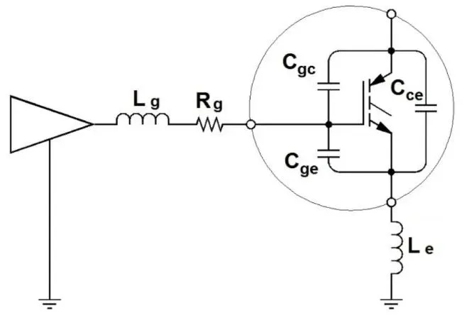
What is the bootstrap capacitor?
The bootstrap capacitor provides the gate-drive voltage needed for the high-side N-channel MOSFET.
When the high-side MOSFET closes, the switch node potential rises close to the input voltage. That raises the MOSFET source above the gate voltage supplied by the gate driver. Without a positive Vgs above the NMOS threshold, the MOSFET cannot conduct. The bootstrap capacitor ensures the gate voltage stays above the source so the high-side device can switch properly.
Consequences of omitting the bootstrap capacitor
Omitting the bootstrap capacitor yields no practical benefit; it is sometimes done to reduce BOM count or by oversight.
If the high-side FET does not fully turn on, the regulator cannot hold the output. The FET will operate in its linear region, dissipating significant power and causing the chip to heat.
To fix this, the designer must add the bootstrap capacitor. If the required value is unclear, use the datasheet example closest to the application. If a device requires a bootstrap capacitor and it is omitted, the regulator will fail to operate correctly. Adding the bootstrap capacitor lets the high-side gate driver drive the FET into saturation so it behaves as a switch and applies the full input to the SW node.
Violating the minimum on-time specification
Designers often choose higher switching frequency to reduce PCB area, at the cost of increased switching losses and reduced efficiency. With a high frequency and a large step-down ratio, the required duty cycle may be forced very small and can fall below the device's minimum on-time. The minimum duty is defined by the relationship shown in Figure 1.
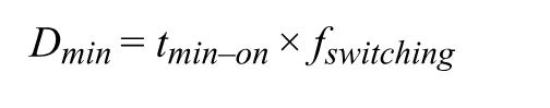
Here, tmin-on is the shortest time the inductor is charged from the input. A switching converter specifies a minimum on-time that must be met so the FET can complete its switching transition.
When on-time falls below the minimum, the inductor discharges faster than it charges within a cycle. At the start of a new cycle the current baseline can be lower than in previous cycles, a phenomenon called current droop. Eventually the inductor current and the output voltage fall so low that the regulator internally increases duty to try to maintain the output.
The reduced inductor ripple appears as increased noise on the output voltage, which can affect sensitive loads and degrade EMI performance.
The primary remedy is to reduce the switching frequency, increasing the absolute on-time. The trade-off is a larger power stage, especially a larger inductor.
Violating the minimum off-time specification
Some applications require a small step-down ratio that can violate the converter's minimum off-time requirement. tmin-off complements tmin-on and is the shortest time the inductor is allowed to be not charged. Like the minimum on-time, the minimum off-time ensures the FET can complete switching transitions and allow normal discharge. When the required duty cycle exceeds the allowed maximum duty (given by Formula 2), the minimum off-time is violated.

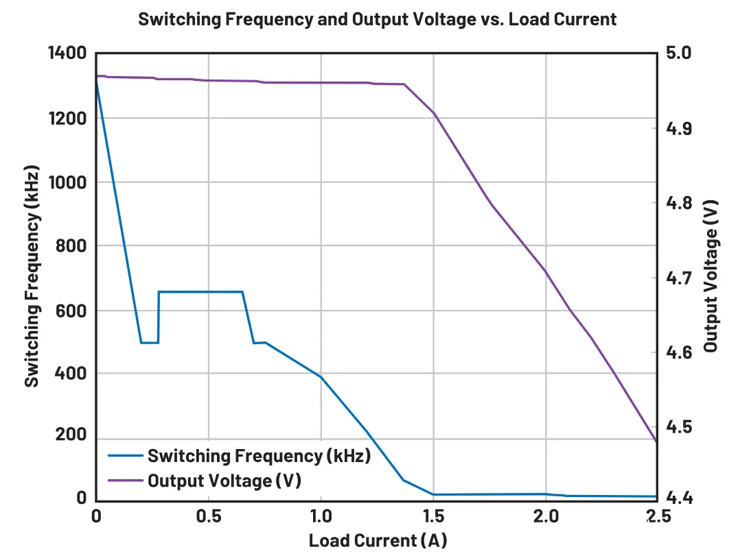
If the duty cycle would exceed the maximum, the SMPS will fold back its operating frequency to avoid violating the minimum off-time. Figure 8 shows this behavior where the device was initially configured for 2 MHz.
Figure 9 shows that as load increases the device reduces its frequency to keep the output regulated. The device runs in discontinuous conduction mode until about 0.28 A, causing the frequency to drop to about 495 kHz then recover to 657 kHz. At 657 kHz the device can regulate up to about 0.7 A before the frequency reduces again until roughly 1.4 A. If the regulator cannot reduce frequency below its specified minimum feedback frequency (in this case 100 kHz), the output voltage will start to fall.
This problem is harder to fix than a minimum on-time violation. Designers are often constrained by required input and output voltages and cannot arbitrarily change duty to lengthen off-time. If a higher input voltage is available, the device can operate at its set frequency because a smaller duty cycle prevents a minimum off-time violation, as shown in Figure 10 with the device running at 2 MHz.
Unlike the minimum on-time case, lowering the switching frequency only helps up to a certain load. If the frequency cannot be reduced enough to avoid the minimum off-time violation, the practical solution is to select a different regulator device that supports higher duty cycles and shorter on-times.
Conclusion
Maintaining proper operation of power transistors is critical. Duty-cycle requirements that are too high or too low can make a switching regulator unstable, causing frequency foldback, output voltage instability, and poor inductor current behavior. Omitting the bootstrap capacitor prevents proper gate drive and can lead to serious faults in the load, FETs, or the regulator itself.