1. What Is GPIO?
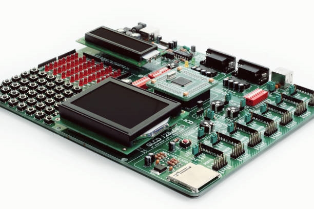
GPIO stands for General Purpose Input Output. Also known as IO ports or bus expanders, GPIOs are composed of pins and functional registers. The packaging and internal structure of GPIOs vary depending on the architecture, including the number of pins and registers. Detailed specifications can be found in the chip's datasheet.
GPIOs are used to control peripheral devices connected to them. Typically, designers refer to schematics to determine where GPIOs are routed on the board, such as to headers or connectors. By connecting peripherals to these points, interaction and control can be achieved through GPIO. At the driver level, interaction occurs via reading and writing the functional registers associated with each GPIO, which changes the state of the connected peripheral.
2. GPIO Architecture
The diagram referenced is based on the STM32F7 series. While GPIO implementations differ across architectures, this example illustrates the concept.
As shown, GPIO in STM32F7 is composed of three main registers and a combination of components: TTL Schottky trigger, diodes, P-MOS transistors, and N-MOS transistors.
3. Working Principle of GPIO
Each GPIO port is connected to a group of pins, such as PA to PG, corresponding to GPIOA, GPIOB, etc. One of these pins typically functions as the output. Essentially, a GPIO pin is a programmable interface, where the CPU can be configured to output a high level on a specific pin via register settings.
The key devices and their functions are as follows:
- Output Data Register: Outputs values through the output driver. Specific bits determine whether P-MOS or N-MOS is used and indicate high/low level. For instance, in a 4-bit register, bits 0-2 define output mode, and bit 3 defines the output signal level: '1' for high, '0' for low.
- P-MOS Transistor: Conducts when Vgs is below a certain threshold. Used in push-pull and open-drain configurations.
- N-MOS Transistor: Conducts when Vgs exceeds a certain threshold. Also used in push-pull and open-drain configurations.
- Protection Diodes: Two diodes are connected to each IO pin to prevent damage from over-voltage or under-voltage. When pin voltage exceeds VDD, the upper diode conducts; when below VSS, the lower diode conducts, protecting the chip from damage.
- TTL Schottky Trigger: Converts current signals into digital signals (0 or 1). Analog inputs bypass this component and require an external ADC for conversion.
The GPIO output mode¡ªpush-pull or open-drain¡ªis implemented using P-MOS and N-MOS transistors. Their behavior differs:
P-MOS vs. N-MOS Characteristics
P-MOS is connected to VDD and has the ability to output high current. Applying a high level turns it on, allowing voltage from the power line to flow. N-MOS, on the other hand, is connected to VSS. It cannot output high level unless an external pull-up resistor is added. When a low level is applied, current flows toward ground.
Therefore, low-level output is usually routed through the N-MOS, which connects to ground, reducing power consumption. In a TTL circuit, high level is defined as >3.4V and low level as <0.2V. Even with no current output, N-MOS remains at a low level.
MOSFET Types
MOSFETs are field-effect transistors, categorized into P-channel and N-channel types depending on whether the source is connected to VDD or VSS.
Push-Pull Output
In push-pull configuration, both high and low levels can be driven. When the output is logic '0', the N-MOS is on and P-MOS is off (high impedance). When the output is logic '1', P-MOS is on and N-MOS is off.
Open-Drain Output
Open-drain configuration can only output low levels. When the output is logic '0', the N-MOS conducts and P-MOS remains off. To output high level, an external pull-up resistor is required on the N-MOS output pin. This ensures undefined signals are pulled high. Open-drain outputs cannot directly drive high levels.
The output circuitry reads the mode bits in the output data register to determine whether to use push-pull or open-drain. In push-pull mode, current comparison via a comparator selects between P-MOS and N-MOS. In open-drain mode, only N-MOS conducts based on logic level. Power efficiency is improved as only one of the two symmetrical power switches conducts at a time, minimizing conduction loss.
Open-drain outputs are typically used in applications requiring strong load-driving capability, such as long-duration operations, due to the presence of the pull-up resistor.
 ALLPCB


