ALLPCB


The TPL0401x-10 device is a single-channel linear-taper digital potentiometer with 128 tap positions. The low terminal is internally tied to GND. The wiper position is adjusted via an I2C serial interface. The TPL0401x-10 is offered in a 6-pin SC70 package and rated for an operating temperature range of -40°C to +125°C. The device has a 10 kΩ end-to-end resistance option and supports a supply voltage range of 2.7 V to 5.5 V. Typical applications include low-power DDR3 reference voltage settings and memory-related calibration.
The low terminal is internally tied to GND.
*Attachment: tpl0401a-10.pdf
Features
- Single channel, 128-step resolution
- 10 kΩ end-to-end resistance option
- Low temperature coefficient: 22 ppm/°C
- I2C serial interface
- Single-supply operation from 2.7 V to 5.5 V
- Resistance tolerance ±20%
- A and B versions with different I2C addresses
- L terminal is internal and connected to GND
- Operating temperature: -40°C to +125°C
- Available in standard SC70 package
- ESD performance per JESD22 tests
- 2000 V human-body model (A114-B, Class II)
Block Diagram
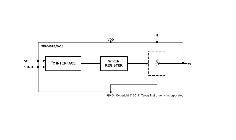
The TPL0401x-10 is a single-channel linear-taper digital potentiometer from Texas Instruments (TI). The series includes TPL0401A-10 and TPL0401B-10 (differing only in I2C address), provides 128-step resolution and 10 kΩ end-to-end resistance, and supports single-supply operation from 2.7 V to 5.5 V. The wiper position is programmed via I2C, making the device suitable for replacing mechanical potentiometers, adjustable power supplies, amplifier gain adjustment, and sensor calibration.
1. Device Overview and Key Specifications
1. Basic Specifications
- Documentation and part numbers: Document SLIS144B, published Sep 2011, revised Feb 2017. TPL0401A-10 I2C address 0101110, TPL0401B-10 address 0111110; pinout and functions are identical.
- Supply and temperature: VDD 2.7 V to 5.5 V. Operating temperature -40°C to 125°C. Storage -65°C to 150°C. Maximum junction temperature 130°C.
- Package and thermal: 6-pin SC70 (2.00 mm × 1.25 mm). Junction-to-ambient thermal resistance 234°C/W. Small form factor for space-constrained applications.
2. Core Performance Metrics
- Resistance and linearity: End-to-end resistance R_TOTAL 8 kΩ to 12 kΩ (typical 10 kΩ). Wiper resistance R_W 35 Ω to 100 Ω. Terminal resistance R_H 100 Ω to 200 Ω. Temperature coefficient 22 ppm/°C for stability across temperature.
- Resolution and accuracy: 128 wiper positions (0x00–0x7F). In voltage-divider mode: INL ±0.5 LSB, DNL ±0.25 LSB. Zero-scale error 0 to 1.5 LSB. Full-scale error -1.5 to 0 LSB.
- Interface and power: Supports I2C standard mode (100 kHz) and fast mode (400 kHz). Standby current I_DD(STBY) up to 1.5 μA across -40°C to 125°C.
- ESD and reliability: Human-body model (HBM) ±2500 V, charged device model (CDM) ±1000 V. Wiper continuous current ±2 mA maximum. Terminal (H/W) maximum ±5 mA.
2. Functional Blocks and Operation
1. Core Functional Blocks
- Single-channel digital potentiometer architecture:
- Includes high terminal (H), wiper terminal (W), and low terminal (L). L is internally grounded, no external connection required. End-to-end resistance is 10 kΩ. The wiper provides 128 discrete positions between H and L for use as a voltage divider or variable resistor.
- Supports two operating modes: voltage-divider mode (using H, W, L; output voltage proportional to wiper position) and rheostat mode (using H-W or W-L variable resistance).
- I2C interface control:
- Wiper position is configured by writing an 8-bit register over I2C. The MSB is discarded on write (for example, writing 0xFF results in 0x7F). The current wiper position can be read back for verification.
- On power-up, the wiper defaults to 0x40 (midscale, 50% divider). There is no nonvolatile memory; after power loss the device returns to the default position.
- Key electrical characteristics:
- Voltage-divider bandwidth 2862 kHz with 10 pF load. Wiper switching settling time 0.152 μs. THD+N 0.03% for good signal integrity.
- Terminal capacitances: H 10 pF, W 11 pF. Low parasitics for higher-frequency applications.
2. Operating Principle
- The device is essentially a digitally controlled resistive network. The host writes wiper positions via I2C to place the wiper at one of 128 taps, changing the resistance ratio between H-W and W-L.
- In voltage-divider mode, V_W = (V_H - V_L) × (D/128), where D is the decimal wiper position (0 ≤ D ≤ 127). Since V_L is fixed to GND, V_W is linearly related to V_H and the wiper position. In rheostat mode, the variable resistance between H-W or W-L is used directly to adjust impedance.
3. Applications and Design Recommendations
1. Typical Applications
- Mechanical potentiometer replacement: Replaces mechanical potentiometers to eliminate wear and contact issues and improve system reliability.
- Adjustable supplies and calibration: Used for reference voltage adjustment, such as DDR3 memory reference calibration, and threshold voltage setting via programmable trimming.
- Amplifier gain and offset adjustment: Paired with operational amplifiers to adjust feedback resistance ratios for gain tuning or fine offset trimming.
- Sensor calibration: Compensates sensor-to-sensor variation by programming the wiper to correct measurement offsets.
2. Design Considerations
- Power-up sequencing: Apply VDD before applying voltages to SDA, SCL, and H/W pins to avoid forward-biasing protection diodes. Wait 120 μs after VDD is stable before initiating I2C communication to ensure the device is ready.
- I2C bus design: Keep SDA and SCL traces as short as practical. Recommended trace width and spacing depend on board design; minimize parasitic capacitance. Use appropriate pull-up resistors on the bus per TI I2C guidelines.
- Layout and decoupling: Place a 0.1 μF to 10 μF decoupling capacitor close to VDD (low ESR recommended) to filter supply ripple. Use low-resistance, low-inductance ground returns. Keep H/W pin routing short to reduce loading effects.
- ESD precautions: The device includes internal ESD protection, but follow standard ESD handling during storage and assembly and avoid leaving pins floating.
4. Key Configuration and Operation
1. Core Configuration
- Wiper programming:
- Write operation: I2C master sends START → slave address (R/W = 0) → ACK → register address (0x00) → ACK → wiper data (0x00–0x7F) → ACK → STOP.
- Read operation: START → slave address (R/W = 0) → ACK → register address (0x00) → ACK → repeated START → slave address (R/W = 1) → ACK → read data → NACK → STOP. Short-read mode is supported by directly sending the read address without a register address.
- Mode selection:
- Voltage-divider mode: Use H, W, and L terminals. Ensure V_H is above V_L (GND). Buffer the output with an op amp if needed to avoid loading the divider and to preserve accuracy.
- Rheostat mode: Use only H-W or W-L terminals. Limit wiper current to ±2 mA to avoid device damage.
2. Important Operational Notes
- After power-up, the wiper defaults to 0x40 (midscale). There is no nonvolatile storage; reprogram the wiper after power-up if a specific initial position is required.
- When writing wiper data, the MSB (bit 7) is discarded. For example, writing 0x80 results in 0x00, and writing 0xFF results in 0x7F.
- In wide temperature applications, account for resistor temperature coefficient. Apply software compensation if necessary to maintain calibration accuracy.