 ALLPCB


If you're looking for clear and practical advice on THT PCB design, including specifics on THT hole size and THT component spacing, you're in the right place. Through-Hole Technology (THT) assembly remains a vital method for creating robust and reliable printed circuit boards (PCBs), especially for applications requiring strong mechanical bonds and high power handling. In this comprehensive guide, we'll walk you through the essential design guidelines and best practices to ensure your THT PCB layout is optimized for manufacturing and performance.
Whether you're an experienced engineer or just starting with PCB design, this blog will cover everything from hole sizing to spacing rules, thermal considerations, and more. Let’s dive into the details of crafting a successful THT PCB layout.
What is Through-Hole Technology (THT) in PCB Design?
Through-Hole Technology, or THT, is a traditional PCB assembly method where component leads are inserted into drilled holes on the board and soldered on the opposite side. Unlike Surface Mount Technology (SMT), which places components directly on the board’s surface, THT provides superior mechanical strength, making it ideal for components that endure physical stress or high currents, such as connectors, transformers, and large capacitors.
THT PCB design is often used in industries like automotive, industrial machinery, and power electronics due to its durability. However, designing for THT assembly requires careful attention to layout details to avoid manufacturing issues and ensure reliability. Let’s explore the key guidelines for effective THT design.
Key Guidelines for THT PCB Design
Creating a successful THT PCB layout involves several critical factors. Below, we break down the most important guidelines to follow, focusing on aspects like THT hole size, THT component spacing, and overall board layout.
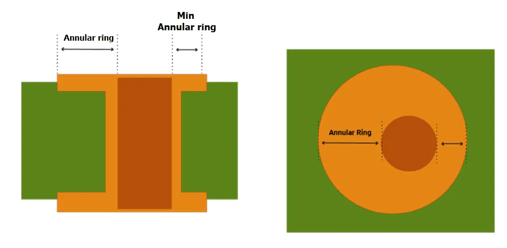
1. Optimizing THT Hole Size for Components
One of the foundational elements of THT PCB design is determining the correct THT hole size for component leads. If the holes are too small, components won't fit properly; if they’re too large, soldering becomes difficult, and the mechanical stability of the joint suffers.
- Standard Hole Sizing: The hole diameter should typically be 0.2 to 0.4 mm larger than the component lead diameter to allow for easy insertion and soldering. For example, a lead with a diameter of 0.6 mm should have a hole size of approximately 0.8 to 1.0 mm.
- Annular Ring Requirements: The annular ring, which is the copper pad surrounding the hole, should be at least 0.25 mm wide on all sides to ensure a strong solder joint. For high-reliability applications, aim for a minimum of 0.3 mm.
- Drill Tolerance: Account for manufacturing tolerances, which can vary by ±0.05 mm. Work with your PCB manufacturer to confirm their drilling capabilities and adjust hole sizes accordingly.
Proper hole sizing reduces the risk of assembly errors and ensures a robust connection between the component and the board.
2. Ensuring Proper THT Component Spacing
THT component spacing is another critical factor in PCB design. Insufficient spacing can lead to soldering issues, thermal problems, or even mechanical interference between components. Here are the best practices for spacing:
- Minimum Spacing Between Components: Maintain at least 2.54 mm (0.1 inches) between adjacent THT components to allow for soldering and to prevent heat buildup during operation. For larger components like electrolytic capacitors, increase this to 5 mm or more.
- Spacing from Board Edge: Keep THT components at least 3 mm away from the board’s edge to avoid damage during handling or mounting.
- Clearance for Wave Soldering: If using wave soldering for assembly, ensure a minimum clearance of 1.5 mm between component bodies to prevent solder bridging.
Adhering to these spacing rules in your THT PCB design helps streamline the assembly process and improves the long-term reliability of the board.
3. Pad Design for Strong Solder Joints
The pad design around THT holes directly impacts the quality of solder joints. A well-designed pad ensures a solid connection and reduces the risk of failures under mechanical or thermal stress.
- Pad Diameter: The pad diameter should be at least 1.5 to 2 times the hole diameter. For a 1.0 mm hole, the pad should be 1.5 to 2.0 mm in diameter.
- Thermal Relief Pads: For components connected to large ground planes, use thermal relief pads with spokes (typically 4) to prevent excessive heat dissipation during soldering. Each spoke should be about 0.3 mm wide.
- Solder Mask Clearance: Ensure the solder mask clearance around pads is at least 0.1 mm larger than the pad itself to avoid mask overlap during manufacturing.
These pad design practices enhance the manufacturability of your PCB and ensure durable solder joints for THT components.
4. Thermal Management in THT PCB Design
THT components often handle high power, which generates heat. Poor thermal management can lead to component failure or reduced lifespan. Consider these strategies in your layout:
- Heat Sinks: For high-power components like voltage regulators, allocate space for heat sinks and ensure proper mounting holes in the layout.
- Copper Pour: Use copper pours or thicker traces (e.g., 2 oz copper or higher) to dissipate heat from power components. Connect these to vias leading to other layers for better heat distribution.
- Component Placement: Place heat-generating THT components away from sensitive parts like microcontrollers or sensors. Maintain at least 5 mm of separation if possible.
Effective thermal management in THT PCB design protects your components and extends the board’s operational life.
5. Trace Width and Routing for THT Components
Routing traces for THT components requires attention to current-carrying capacity and signal integrity. Since THT designs often involve high-power applications, trace width is especially important.
- Trace Width for Current: Use a trace width calculator to determine the appropriate width based on current. For instance, a 1 Amp current at 1 oz copper thickness requires a trace width of about 0.5 mm, while 5 Amps may need 2.5 mm or more.
- Routing Clearance: Maintain a minimum clearance of 0.2 mm between traces to prevent short circuits, increasing to 0.5 mm or more for high-voltage designs (above 50V).
- Avoid Sharp Angles: Route traces at 45-degree angles rather than 90-degree turns to minimize signal reflection and manufacturing issues.
Proper trace design ensures that your THT PCB can handle the required power without overheating or signal degradation.
6. Considerations for Automated Assembly
Many THT assemblies use automated insertion machines for component placement. Designing with automation in mind can reduce errors and speed up production.
- Component Orientation: Align polarized components like diodes and capacitors in the same direction to simplify automated insertion.
- Hole and Pad Consistency: Ensure all holes and pads conform to standard sizes for the insertion equipment. Non-standard sizes can cause delays or require manual assembly.
- Panelization: If producing multiple boards, design with panelization in mind, leaving at least 5 mm between individual PCBs for easy separation after assembly.
Designing for automation can significantly improve the efficiency of your THT assembly process.
Common Mistakes to Avoid in THT PCB Design
Even with careful planning, certain pitfalls can compromise a THT PCB layout. Here are some common mistakes to watch out for:
- Incorrect Hole Sizes: Using holes that are too tight or too loose for component leads can lead to assembly issues or weak solder joints. Always double-check lead diameters against hole sizes.
- Insufficient Spacing: Crowding components too closely can cause soldering defects or thermal issues. Stick to recommended THT component spacing guidelines.
- Ignoring Thermal Needs: Failing to account for heat dissipation in high-power designs can result in component failure. Always include thermal reliefs and adequate copper areas.
- Poor Pad Design: Small or improperly shaped pads can weaken solder joints. Ensure pads are large enough and properly connected to planes or traces.
Avoiding these errors will save time and cost during manufacturing and improve the reliability of your PCB.
Advantages of THT in Modern PCB Design
While SMT dominates much of today’s electronics due to its compactness, THT still offers unique benefits that make it indispensable in certain applications:
- Mechanical Strength: THT components are physically anchored through the board, providing excellent resistance to vibration and shock, ideal for automotive or industrial environments.
- High Power Handling: THT is better suited for components that handle high currents or voltages, such as power supplies or motor controllers.
- Ease of Repair: THT components are easier to replace or rework manually compared to tiny SMT parts, making them a preferred choice for prototypes or repairable designs.
Understanding these advantages helps in deciding when to use THT over other assembly methods in your PCB projects.
Conclusion: Mastering THT PCB Design for Reliable Boards
Designing a PCB for Through-Hole Technology assembly requires precision and attention to detail, from selecting the correct THT hole size to ensuring proper THT component spacing. By following the best practices outlined in this guide—such as optimizing pad design, managing thermal issues, and routing traces effectively—you can create a THT PCB layout that is both manufacturable and reliable.
Whether you're working on a high-power industrial application or a prototype that needs durability, these THT PCB design guidelines will help you achieve a successful outcome. Focus on the specifics, collaborate with your manufacturing partner for tolerances and capabilities, and always double-check your layout against these standards.
With these strategies in hand, you're well-equipped to tackle your next THT assembly project with confidence and precision.


