 ALLPCB


If you're looking to enhance your PCB design with high-density interconnects (HDI) while maintaining signal integrity, understanding blind vias, buried vias, and controlled depth drilling (often referred to as back drilling) is essential. These techniques allow for more compact designs, reduced signal interference, and improved performance in modern electronics. In this comprehensive guide, we'll dive deep into what blind and buried vias are, how controlled depth drilling works, and why these methods are critical for HDI PCBs and signal integrity. Whether you're an engineer or a designer, this post will equip you with actionable insights to optimize your next project.
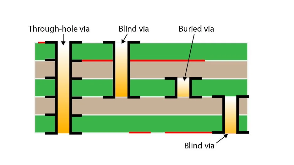
What Are Blind and Buried Vias in PCB Design?
Blind and buried vias are specialized types of vertical interconnects used in multilayer printed circuit boards (PCBs) to connect different layers without occupying unnecessary space or interfering with outer layers. Unlike standard through-hole vias that pass through the entire board, these vias are designed for specific layer connections, making them ideal for high-density designs.
Blind Vias: These connect the outermost layer of a PCB to one or more inner layers but do not extend through the entire board. For example, a blind via might link the top layer to the second layer in a six-layer board without reaching the bottom layer. This saves space and reduces the risk of signal interference on unused layers.
Buried Vias: These are located entirely within the internal layers of a PCB, connecting two or more inner layers without reaching the outer surfaces. Since they are hidden inside the board, buried vias free up space on the outer layers for additional components or traces.
Both types of vias are crucial in HDI PCBs, where space is limited, and wiring density is high. They help reduce the board's overall size while maintaining functionality, often used in compact devices like smartphones and medical equipment.
Why Use Blind and Buried Vias in HDI PCBs?
High-density interconnect (HDI) PCBs are designed to pack more functionality into smaller spaces. Blind and buried vias play a pivotal role in achieving this by offering several benefits:
- Increased Wiring Density: By limiting vias to specific layers, more traces and components can fit on the board. This is vital for devices where every square millimeter counts.
- Reduced Signal Interference: Shorter via lengths minimize signal reflections and crosstalk, improving signal integrity. For high-speed designs, this can mean the difference between a functional board and one plagued by noise.
- Smaller Board Size: With vias confined to necessary layers, the overall footprint of the PCB can be reduced, saving material costs and fitting into tighter enclosures.
- Enhanced Design Flexibility: Designers can place components and routes more efficiently, optimizing the layout for performance and manufacturability.
For instance, in a typical HDI PCB with 8 layers, using blind vias to connect layers 1 to 2 and buried vias between layers 3 to 5 can reduce via stubs (unused via portions) that degrade signal quality at frequencies above 5 GHz.
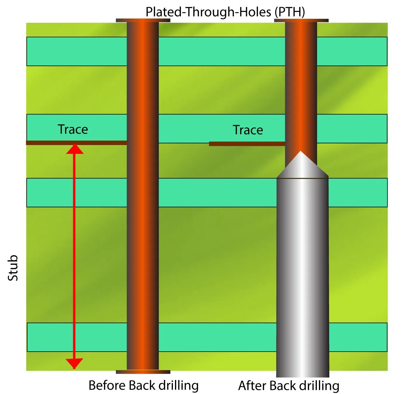
What Is Controlled Depth Drilling (Back Drilling) in PCB Design?
Controlled depth drilling, commonly known as back drilling, is a manufacturing technique used to remove unused portions of via barrels in multilayer PCBs. When a via extends beyond the layers it needs to connect, the leftover stub can act as an antenna, causing signal reflections and degrading signal integrity, especially in high-speed designs.
Back drilling involves using a specialized drill to remove the excess via stub after the initial plating process. The drill is precisely controlled to stop at a specific depth, ensuring that only the necessary conductive path remains. This process is often applied to through-hole vias in HDI PCBs to mimic the benefits of blind vias without the added manufacturing complexity.
For example, in a 10-layer PCB, a through-hole via connecting layers 1 to 4 might leave a stub from layers 5 to 10. Back drilling removes this stub, reducing signal distortion for data rates exceeding 10 Gbps.
How Controlled Depth Drilling Improves Signal Integrity
Signal integrity is a critical concern in modern PCB design, especially for high-speed applications like telecommunications and data centers. Via stubs left in through-hole vias can cause significant issues, such as:
- Signal Reflections: Stubs create impedance mismatches, leading to reflections that interfere with the main signal. This can result in data errors or reduced transmission speeds.
- Resonance: At certain frequencies, stubs can resonate, amplifying noise and further degrading performance.
- Crosstalk: Unwanted coupling between adjacent signals can occur due to stub effects, impacting overall system reliability.
Controlled depth drilling addresses these issues by physically removing the stub, ensuring a cleaner signal path. Studies have shown that back drilling can reduce signal loss by up to 20% in high-speed designs operating at 25 Gbps or higher. It also lowers the risk of electromagnetic interference (EMI), making it a preferred technique for applications requiring strict signal quality standards.
Applications of Blind and Buried Vias with Back Drilling
The combination of blind vias, buried vias, and controlled depth drilling is widely used across industries where compact, high-performance PCBs are needed. Some key applications include:
- Consumer Electronics: Devices like smartphones and wearables rely on HDI PCBs with blind and buried vias to fit complex circuitry into tiny form factors.
- Telecommunications: High-speed data transmission equipment, such as routers and switches, use back drilling to maintain signal integrity at multi-gigabit speeds.
- Medical Devices: Compact and reliable PCBs are critical for equipment like pacemakers and imaging systems, where space and performance are non-negotiable.
- Automotive Systems: Advanced driver-assistance systems (ADAS) and infotainment units benefit from HDI designs to handle high-speed signals and dense layouts.
In these scenarios, the use of blind and buried vias can increase component density by up to 30%, while back drilling ensures that signal quality remains intact even under demanding conditions.
Manufacturing Considerations for Blind and Buried Vias
While blind and buried vias offer significant advantages, they come with unique manufacturing challenges that must be considered during the design phase:
- Precision Drilling: Blind vias are often created using laser drilling for smaller diameters (typically 3 to 6 mils), while buried vias require sequential lamination processes, adding to production complexity.
- Cost Implications: The additional steps involved in creating these vias and performing back drilling can increase manufacturing costs by 15-25% compared to standard through-hole designs.
- Design Rules: Designers must adhere to strict aspect ratios (via depth to diameter) to ensure reliability. For instance, a common rule is to keep the aspect ratio below 1:1 for blind vias to avoid plating issues.
Working with a trusted PCB manufacturer who understands these requirements is crucial to achieving a successful design without unexpected delays or defects.
Design Tips for Optimizing Blind and Buried Vias in HDI PCBs
To make the most of blind and buried vias while ensuring signal integrity, consider the following design tips:
- Minimize Via Stubs: Use back drilling wherever possible to eliminate stubs in through-hole vias, especially for signals operating above 5 GHz.
- Optimize Layer Stackup: Plan your layer stackup to group high-speed signals on adjacent layers, reducing the need for long vias and minimizing signal loss.
- Use Microvias for HDI: For ultra-dense designs, incorporate microvias (small-diameter blind vias) to connect outer layers to the first inner layer, keeping impedance consistent.
- Simulate Signal Performance: Use simulation tools to model signal behavior and identify potential issues like reflections or crosstalk before manufacturing.
- Follow Manufacturing Guidelines: Check with your PCB fabricator for specific design constraints, such as minimum via sizes or drilling tolerances, to avoid production issues.
By carefully planning via placement and leveraging controlled depth drilling, you can achieve a balance between density and performance in your PCB designs.
Challenges and Limitations of Controlled Depth Drilling
While back drilling is a powerful technique for improving signal integrity, it’s not without challenges:
- Precision Requirements: Drilling must be accurate to within a few mils to avoid damaging necessary via portions. A deviation of just 0.1 mm can render a via unusable.
- Increased Costs: The specialized equipment and additional manufacturing steps can raise costs, especially for large production runs.
- Design Complexity: Back drilling requires careful planning to ensure that drill depths align with layer connections, adding to the design workload.
Despite these challenges, the benefits of improved signal integrity often outweigh the drawbacks for high-speed and high-density applications.
How to Choose Between Blind Vias, Buried Vias, and Back Drilling
Deciding which via type or drilling method to use depends on your project’s specific needs:
- Use Blind Vias when you need to connect outer layers to inner layers without penetrating the entire board. They’re ideal for HDI designs with limited space on the bottom layer.
- Use Buried Vias for internal layer connections where outer layer space is at a premium. They work well in multilayer boards with complex internal routing.
- Use Back Drilling for through-hole vias in high-speed designs where signal integrity is critical. It’s a cost-effective alternative to blind vias in some cases.
For a mixed approach, many HDI PCBs combine all three techniques to optimize space, cost, and performance. For example, a 12-layer board might use blind vias for outer connections, buried vias for internal routing, and back drilling for high-speed signal paths.
Future Trends in Via Technology for PCB Design
As electronics continue to shrink and performance demands grow, via technology is evolving. Some emerging trends include:
- Stacked Microvias: Multiple microvias stacked on top of each other to connect more layers in HDI PCBs, further increasing density.
- Advanced Materials: New dielectric materials with lower loss tangents to support high-frequency signals through vias.
- Automated Drilling Techniques: Improved precision in controlled depth drilling with AI-driven systems to reduce errors and costs.
Staying updated on these advancements can help you future-proof your designs and maintain a competitive edge in PCB development.
Conclusion: Mastering Vias and Drilling for Better PCB Performance
Blind vias, buried vias, and controlled depth drilling are game-changers in the world of PCB design, especially for HDI applications where space and signal integrity are paramount. By understanding how these techniques work and applying them strategically, you can create compact, high-performance boards that meet the demands of modern electronics. From reducing signal reflections with back drilling to maximizing wiring density with blind and buried vias, these methods offer practical solutions for engineers and designers alike.
Whether you're working on consumer gadgets, telecom equipment, or automotive systems, mastering these via technologies will elevate your designs. Partner with a reliable PCB manufacturer to ensure precision in drilling and fabrication, and always simulate your designs to catch potential issues early. With the right approach, your next project can achieve both efficiency and excellence.


