ALLPCB


Introduction
For many embedded engineers, the journey into the field begins with foundational platforms like 8051-based microcontrollers or the widely-used STM32 series. STMicroelectronics has a strong foundation in MCU chip research, development, and market presence, making the STM32 family a familiar name in the industry.
Historically, most engineers viewed STM32 devices strictly as microcontrollers (MCUs). This perception was accurate until around 2019, when ST began to shift its strategy, expanding the STM32 portfolio from MCUs toward general-purpose microprocessors (MPUs). A key milestone in this transition was the launch of the dual-core heterogeneous STM32MP157, which was quickly adopted by several development board manufacturers.
This raises the question: Why has the performance of the STM32 family scaled so dramatically, from the original 72 MHz STM32F1 to the 1.5 GHz STM32MP257?
Market Demands Driving Performance Gains
The primary driver behind this evolution is the significant change in the embedded market, fueled by rapid advancements in Artificial Intelligence (AI), the Internet of Things (IoT), industrial automation, and smart devices. These applications place increasingly stringent demands on chip capabilities.
During chip selection, engineers now frequently require a combination of high computing power, real-time performance, large storage capacity, high integration, and low power consumption, often within a single-chip solution.
In response, the STM32 portfolio has advanced significantly. Recent MPU iterations, such as the STM32MP257, now integrate Neural Processing Units (NPUs), delivering a substantial leap in overall performance.
Example Platform: The STM32MP257
A new development board, the ATK-DLMP257B, exemplifies this trend. It is designed as a comprehensive platform for project evaluation, featuring a wide array of peripheral interfaces to explore the full potential of its core processor.
The board's core module is built around the STM32MP257DAK3, a multi-core heterogeneous MPU with the following specifications:
- Dual-core Arm Cortex-A35 at 1.5 GHz
- Single-core Arm Cortex-M3 at 400 MHz
- NPU with 1.35 TOPS of compute power
- Multimedia GPU at 900 MHz
To facilitate thorough testing and performance evaluation, the baseboard provides an extensive set of interfaces, including:
- Audio: Dual-channel speaker and headphone jacks
- Display: MIPI-DSI, LVDS, and RGB-LCD
- Camera: MIPI-CSI
- Wireless: Wi-Fi, Bluetooth, and 4G
- Wired Networking: 3x Gigabit Ethernet ports
- Industrial: 3x CAN-FD interfaces
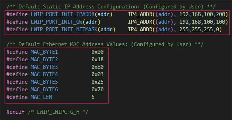
Software and Ecosystem
The ATK-DLMP257B development board ships with a pre-loaded UI demo program that showcases the chip's multimedia processing capabilities. The entire UI is developed using Qt, and its source code is available in the board's documentation under the GPL V3 license for developers to use and modify.
Platforms like this are typically aimed at two main groups: enterprise users developing product prototypes and embedded engineers seeking to transition into AI applications. The combination of ST's robust hardware and software ecosystem and the availability of comprehensive tutorials can help lower the barrier to entry for embedded AI development.