 ALLPCB


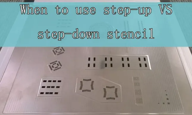
Are you struggling to get the right amount of solder paste for different components on your printed circuit board (PCB)? Step-up stencils are the solution to increase volume for component solder paste, especially for larger parts that need stronger connections. These specialized tools make easy stencil application a reality, ensuring precise soldering in high-density PCB assembly. In this detailed guide, we'll explore how step-up stencils work, their benefits, and practical tips for using them effectively in your manufacturing process.
What Are Step-Up Stencils and Why Do They Matter?
In surface mount technology (SMT) assembly, applying the correct amount of solder paste is critical for creating reliable electrical and mechanical connections. Standard stencils have a uniform thickness, which can be problematic when a PCB has components of varying sizes. Small components, like 0402 resistors (measuring just 1.0mm x 0.5mm), need less paste to avoid bridging, while larger components, such as I/O connectors or power modules, require more paste for durability under external stress.
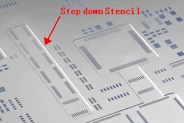
Step-up stencils address this challenge by featuring areas of increased thickness. These "stepped" regions allow for a higher volume of solder paste to be deposited where needed, ensuring optimal soldering results across diverse components on the same board. By using step-up stencils, manufacturers can avoid defects like insufficient solder joints or excess paste spillage, making the process more efficient and reliable.
How Step-Up Stencils Increase Volume for Component Solder Paste
The primary advantage of step-up stencils is their ability to increase the volume of solder paste in specific areas. This is achieved through a design where certain sections of the stencil are thicker—typically by 0.025mm to 0.05mm compared to the base thickness. For example, a standard stencil might be 0.1mm thick, while the stepped-up area for larger components could be 0.15mm thick. This difference allows more paste to be pushed through the apertures during application, creating stronger solder joints for components that need it.
For power-related components or connectors exposed to frequent plugging and unplugging, this extra solder volume is essential. Insufficient solder can lead to joint failure under mechanical stress, causing reliability issues. Step-up stencils ensure that these components receive the necessary paste volume—often up to 50% more than what a standard stencil would provide—without affecting nearby smaller components that require less paste.
Benefits of Using Step-Up Stencils in PCB Assembly
Step-up stencils offer several advantages that make them a valuable tool for modern PCB manufacturing. Here are some key benefits:
- Precision in Solder Paste Volume: By tailoring the stencil thickness to component needs, step-up stencils ensure that each part gets the exact amount of paste required. This reduces defects like open joints or solder bridges.
- Improved Reliability: Components with higher mechanical stress, such as connectors, benefit from stronger solder joints due to the increased paste volume, enhancing the overall durability of the PCB.
- Cost Efficiency: Using a single step-up stencil instead of multiple stencils or manual paste application saves time and reduces production costs. It streamlines the assembly process, especially for complex boards with mixed component sizes.
- Compatibility with High-Density Designs: Modern PCBs often pack small and large components into tight spaces. Step-up stencils handle these mixed requirements without compromising on quality.
Easy Stencil Application with Step-Up Stencils
One of the standout features of step-up stencils is their ease of use. Despite their specialized design, they integrate seamlessly into standard SMT assembly processes. Here's how easy stencil application works with step-up stencils:
- Design and Fabrication: The stencil is custom-designed based on the PCB layout. Areas requiring more solder paste are identified during the design phase, and the stencil is manufactured with stepped regions using precision laser cutting or chemical etching. Typical base thicknesses range from 0.08mm to 0.12mm, with step-up areas increasing by 0.02mm to 0.05mm.
- Alignment: The stencil is aligned with the PCB using fiducial marks or automated vision systems in stencil printers. Proper alignment ensures that the stepped areas correspond accurately to the components needing more paste.
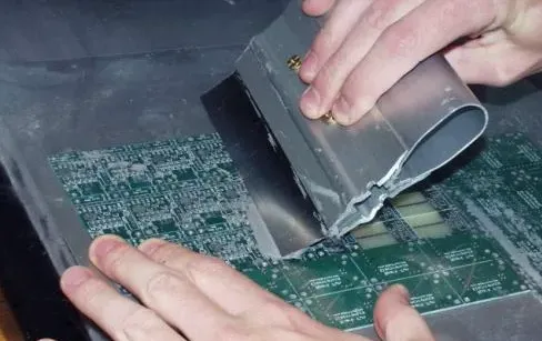
- Paste Application: Solder paste is applied using a squeegee, just like with standard stencils. The thicker step-up areas naturally allow more paste to be deposited, while thinner areas limit the volume for smaller components.
- Inspection: After application, automated optical inspection (AOI) systems can verify the paste volume and placement, ensuring consistency across the board.
The process is straightforward and doesn't require significant changes to existing equipment or workflows. This makes step-up stencils an accessible solution for manufacturers looking to optimize solder paste application without overhauling their setup.
Practical Tips for Implementing Step-Up Stencils
To get the most out of step-up stencils and ensure easy stencil application, consider the following practical tips:
- Work with Accurate Design Data: Provide detailed Gerber files and component specifications to the stencil manufacturer. Clearly indicate which components need increased solder paste volume to avoid errors in the step-up design.
- Choose the Right Thickness: Select a base stencil thickness that suits the majority of components (e.g., 0.1mm for fine-pitch parts). Then, determine the step-up thickness based on the needs of larger components—typically an increase of 25-50% in thickness works well.
- Optimize Aperture Design: Ensure that the apertures in the stepped areas are sized correctly to release the increased paste volume without clogging. A common guideline is to maintain an area ratio (aperture opening to wall thickness) of at least 0.66 for proper paste transfer.
- Use Quality Solder Paste: The viscosity and particle size of the solder paste should match the stencil design. Type 4 or Type 5 pastes, with smaller particle sizes (15-25 micrometers), are often ideal for fine-pitch components, while Type 3 (25-45 micrometers) may suit larger apertures in stepped areas.
- Maintain Stencil Cleanliness: Regularly clean the stencil to prevent paste buildup, especially in the stepped regions where more material is deposited. Use automated under-stencil wiping systems for consistent results during high-volume production.
Challenges and Solutions with Step-Up Stencils
While step-up stencils are highly effective, they do come with some challenges. Understanding these potential issues and their solutions can help ensure a smooth implementation:
- Challenge - Manufacturing Complexity: Creating a stencil with varying thicknesses requires advanced fabrication techniques, which can increase lead times and costs compared to standard stencils.
Solution: Partner with a reliable stencil supplier who uses precision laser cutting to produce high-quality step-up stencils efficiently. Bulk ordering can also reduce per-unit costs. - Challenge - Paste Release Issues: Thicker areas may experience poor paste release if the aperture design isn’t optimized, leading to inconsistent deposits.
Solution: Work with engineers to fine-tune the aperture size and shape. Testing different designs during the prototype phase can help identify the best configuration. - Challenge - Compatibility with Printers: Some older stencil printers may struggle with the uneven surface of step-up stencils, affecting paste application uniformity.
Solution: Upgrade to modern printers with adjustable squeegee pressure and automated alignment features to accommodate stepped designs.
Real-World Applications of Step-Up Stencils
Step-up stencils are widely used in industries where PCB reliability is paramount. For instance, in automotive electronics, PCBs often include power modules and connectors that endure vibration and thermal stress. Step-up stencils ensure these components receive sufficient solder paste for robust joints, reducing the risk of failure in harsh environments.
In consumer electronics, such as smartphones and tablets, high-density boards combine tiny passives (like 0201 capacitors, measuring 0.6mm x 0.3mm) with larger chips and connectors. Step-up stencils allow manufacturers to apply the right paste volume to each component, maintaining signal integrity and mechanical strength without compromising on space efficiency.
Conclusion: Elevate Your PCB Assembly with Step-Up Stencils
Step-up stencils are a game-changer for PCB assembly, offering a practical way to increase volume for component solder paste where it’s needed most. Their ability to tailor solder paste deposition to specific components ensures stronger joints, fewer defects, and higher reliability—especially for complex, high-density designs. With easy stencil application and compatibility with standard SMT processes, they’re an accessible solution for manufacturers aiming to optimize their production.
By understanding how step-up stencils work and following best practices for their use, you can streamline your assembly process and achieve consistent, high-quality results. Whether you're working on automotive, consumer, or industrial electronics, integrating step-up stencils into your workflow can make a significant difference in performance and efficiency.


