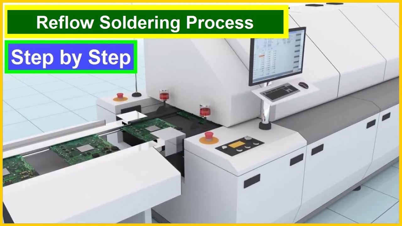
Are you looking for a detailed guide on the selective soldering process flow? Whether you're new to electronics manufacturing or a seasoned professional, understanding the step-by-step soldering guide, from preparation for selective soldering to the final inspection of solder joints, is crucial for achieving high-quality results. In this comprehensive blog, we’ll walk you through every stage of the process, including a soldering quality checklist to ensure your work meets industry standards.
Selective soldering is a precise technique used in electronics manufacturing to solder specific through-hole components on a printed circuit board (PCB) without affecting nearby areas. It’s ideal for mixed-technology boards where surface-mount components are already in place. By following this guide, you’ll learn how to execute the process effectively and ensure top-notch solder joint quality. Let’s dive into the details of each step!
What Is Selective Soldering and Why Is It Important?
Selective soldering is a specialized soldering method that targets individual through-hole components on a PCB using a localized solder fountain or nozzle. Unlike wave soldering, which solders all components at once, selective soldering offers precision, making it perfect for complex boards with a mix of through-hole and surface-mount components. This process minimizes thermal stress on sensitive parts and reduces the risk of defects.
The importance of mastering the selective soldering process flow lies in its ability to improve production efficiency and product reliability. With the right preparation for selective soldering and attention to detail during the final inspection of solder joints, manufacturers can achieve consistent, high-quality results. This is especially critical in industries like automotive, medical, and aerospace, where reliability is non-negotiable.
Step 1: Preparation for Selective Soldering
The foundation of a successful selective soldering process begins with thorough preparation. Proper planning and setup can prevent costly errors down the line. Here’s how to get started with preparation for selective soldering:
- Design Review: Ensure the PCB layout is optimized for selective soldering. Keep a minimum clearance of 3 mm between components to avoid solder bridging. Check that through-hole components are positioned for easy access by the soldering nozzle.
- Component Selection: Verify that the components are suitable for selective soldering. Confirm their thermal tolerance, as the process involves localized heating up to 300°C.
- Solder Mask and Flux Application: Apply a high-quality solder mask to protect areas that shouldn’t be soldered. Use a no-clean flux or a water-soluble flux, depending on your cleaning process, to promote better solder wetting.
- Equipment Setup: Calibrate the selective soldering machine to match the board’s requirements. Set the solder temperature (typically 260°C to 300°C) and nozzle size based on the component lead diameter, usually ranging from 3 mm to 12 mm.
Step 2: Preheating the PCB
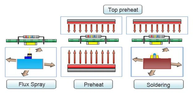
Preheating is a critical step in the selective soldering process flow to ensure uniform temperature distribution and prevent thermal shock. Here’s how it works:
- Temperature Setting: Preheat the PCB to a temperature between 100°C and 150°C, depending on the board material and component specifications. This reduces the thermal gradient during soldering.
- Duration: Allow 1 to 3 minutes for preheating to ensure the entire board reaches a stable temperature. Larger or thicker boards may require longer times.
- Equipment: Use an infrared or convection preheating system integrated into the selective soldering machine for consistent results.
Proper preheating minimizes defects like cold solder joints and ensures better solder flow. Skipping or rushing this step can lead to poor adhesion and component damage.
Step 3: Flux Application for Precision
Flux application is essential to clean the surfaces of the leads and pads, ensuring proper solder wetting. Follow these steps for effective fluxing:
- Type of Flux: Choose a flux compatible with your solder alloy, such as rosin-based or no-clean flux. For high-reliability applications, consider water-soluble flux for easier cleaning.
- Application Method: Use a precision spray or drop-jet system to apply flux only to the targeted areas. Avoid excessive flux, as it can cause residue buildup.
- Drying Time: Allow the flux to activate for 10 to 30 seconds before soldering. Some systems combine preheating and flux drying for efficiency.
Step 4: Selective Soldering Execution
Now it’s time to perform the actual soldering. This step requires precision and control to achieve strong, reliable joints. Here’s a step-by-step soldering guide for this stage:
- Solder Bath Setup: Maintain the solder bath at a consistent temperature, typically 260°C for lead-free solder alloys like SAC305. Monitor the solder level to avoid overflow or insufficient coverage.
- Nozzle Positioning: Program the machine to position the solder nozzle directly under the targeted through-hole component. The nozzle diameter should match the lead size for optimal flow.
- Soldering Time: Apply solder for 2 to 5 seconds per joint, depending on the component and board thickness. Longer dwell times may be needed for larger leads or multilayer boards.
- Nitrogen Atmosphere: Use a nitrogen environment around the solder nozzle to reduce oxidation and improve joint quality. Maintain nitrogen purity above 99.99% for best results.
This stage is where precision matters most. A well-executed selective soldering process flow reduces defects like insufficient fill or solder bridges, ensuring reliable connections.
Step 5: Cooling and Cleaning
After soldering, proper cooling and cleaning are necessary to solidify the joints and remove any residues. Here’s how to handle this step:
- Cooling: Allow the PCB to cool gradually at room temperature or use forced air cooling to prevent thermal stress. Rapid cooling can cause cracks in the solder joints.
- Cleaning: If using water-soluble flux, clean the board with deionized water at 40°C to 60°C to remove residues. For no-clean flux, inspect for visible residues and clean only if necessary to avoid damaging components.
Proper cooling and cleaning preserve the integrity of the solder joints and prepare the board for inspection.
Step 6: Final Inspection of Solder Joints
The final inspection of solder joints is a critical step to ensure the quality and reliability of the soldered connections. This stage involves both visual and automated checks to identify defects. Follow these guidelines:
- Visual Inspection: Use a magnifying glass or microscope (10x to 20x magnification) to check for defects like insufficient solder fill, bridging, or cracks. Look for a smooth, shiny finish on the joints, indicating proper wetting.
- Automated Optical Inspection (AOI): Employ AOI systems to scan for inconsistencies in solder joint shape and size. These systems can detect defects at a resolution of 10 microns or better.
- X-Ray Inspection: For multilayer boards, use X-ray inspection to check for hidden defects like voids or incomplete barrel fill in through-hole joints. Aim for a void percentage of less than 25% per industry standards like IPC-A-610.
Soldering Quality Checklist for Perfection
To ensure every solder joint meets the required standards, use this soldering quality checklist during the final inspection. This checklist helps identify issues early and maintain consistency across production runs:
- Solder Coverage: Confirm that the solder covers at least 75% of the through-hole barrel height for adequate mechanical strength.
- Wetting Quality: Check for complete wetting of the component lead and pad, with a concave fillet shape indicating a strong bond.
- No Bridging: Ensure there are no unintended connections between adjacent pins or pads.
- No Voids or Cracks: Verify that solder joints are free of voids (less than 25% by volume) and cracks that could compromise reliability.
- Component Alignment: Confirm that components are aligned correctly and not tilted or lifted due to uneven soldering.
- Residue Check: Ensure no flux or solder residue remains on the board, especially in high-reliability applications.
Adhering to this soldering quality checklist ensures that your PCBs meet industry standards and perform reliably in their intended applications.
Common Challenges and Solutions in Selective Soldering
Even with a well-defined selective soldering process flow, challenges can arise. Here are some common issues and how to address them:
- Insufficient Solder Fill: This can occur due to low solder temperature or inadequate flux. Increase the solder bath temperature by 5°C to 10°C or adjust flux application for better wetting.
- Solder Bridging: Often caused by excessive solder or poor nozzle positioning. Reduce dwell time by 1 to 2 seconds and recalibrate the nozzle alignment.
- Thermal Damage: Prolonged exposure to heat can damage components. Shorten soldering time or lower preheating temperature to stay within component tolerances.
By anticipating these issues and applying the right solutions, you can maintain high-quality output throughout the process.
Conclusion: Mastering the Selective Soldering Process
The selective soldering process flow is a powerful method for achieving precise, reliable solder joints on complex PCBs. From meticulous preparation for selective soldering to the detailed final inspection of solder joints, each step plays a vital role in ensuring quality. By following this step-by-step soldering guide and using the soldering quality checklist, you can minimize defects and produce boards that meet the highest standards.
Whether you’re soldering a small batch or scaling up for mass production, attention to detail at every stage—from preheating and fluxing to cooling and inspection—will set you up for success. With practice and adherence to best practices, selective soldering can become a seamless part of your manufacturing process, delivering consistent results every time.
 ALLPCB


