ALLPCB


Understanding EMC
Electromagnetic compatibility (EMC) is the study of the unintentional generation, propagation, and reception of electromagnetic energy, and the undesirable effects that such energy may cause. The goal of EMC is to ensure that different electronic devices can operate correctly in the same environment without producing an intolerable level of electromagnetic interference for any other device in that environment.
Common Units for Electromagnetic Disturbance
The decibel (dB) is a common unit for expressing disturbance levels. The original definition of a decibel is the ratio of two power levels.
The unit dBm is often used to express power, representing the power level relative to 1 mW.
The unit dBuV is used to express voltage, representing the voltage level relative to 1 uV.
Radiated disturbances are typically measured by electromagnetic field strength, with the unit V/m. A common unit is dBuV/m.
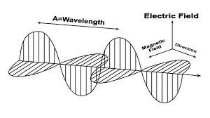
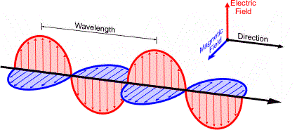
When a signal propagates along a transmission line, an electric field is generated between the signal path and the return path. A magnetic field also surrounds both paths. For a 50Ω microstrip line on an FR4 substrate, the electric and magnetic field lines are not confined directly beneath the microstrip but extend into the surrounding space. These extending fields are known as fringing fields.
Inductive Coupling Suppression Methods
- Minimize the magnitude and rate of change of current in the interfering source circuit.
- Ensure the victim circuit has a high impedance.
- Reduce the mutual inductance between the two systems. To do this, keep wires as short as possible, maximize the distance between them, avoid parallel routing, and minimize the loop area when using two-wire structures (e.g., twisted pairs).
- Use magnetic shielding for the interference source or the victim to suppress the interfering magnetic field.
- Employ balancing techniques to cancel out most of the interfering magnetic field and the coupled noise signals. For example, orient the victim conductor loop to minimize the cutting of magnetic field lines (i.e., loop plane parallel to the field lines) to minimize coupled noise. Additionally, twisting the wires of the interference source can help cancel out the magnetic fields generated by the currents.
Radiated Interference
Near-Field and Far-Field
Interference transmitted through space is essentially the propagation of electromagnetic energy from a source in the form of fields. These fields are categorized as near-field (or induction field) and far-field (or radiation field). The criterion for distinguishing them is the distance (r) from the source.
r > λ/2π is the far-field.
r < λ/2π is the near-field.
We use wave impedance to describe the relationship between the electric field (E) and magnetic field (H). Wave impedance is defined as:
Z? = E/H
In the far-field, the electric and magnetic fields are perpendicular to each other and to the direction of propagation, forming a plane wave. The ratio of E to H is a constant value, the impedance of free space: Z? = 120π ≈ 377 Ω. The relationship between wave impedance and distance is shown in the wave impedance graph.
PCB vs. Cable Radiation
1. PCB Radiation
A PCB contains many signal loops, including differential-mode and common-mode current loops. To calculate their radiated intensity, they can be modeled as loop antennas, with the radiation intensity calculated by the following formula:
2. Cable Radiation
To calculate the radiation intensity from a cable, it is modeled as a monopole antenna. Its radiation intensity is calculated by the following formula:
These two formulas show that the radiation efficiency of a cable is much higher than that of a PCB.
Electromagnetic Shielding Theory
1. The Concept of Shielding Effectiveness
Shielding is a technique that uses a conductive enclosure (a shield) to block or reduce the transmission of electromagnetic energy. It is a primary method for suppressing EMI. Shielding has two main purposes: to limit the leakage of internally generated electromagnetic energy and to prevent external radiated interference from entering a specific area.
When an electromagnetic field passes through a metallic material, its strength is significantly reduced. This phenomenon is the shielding effect of the material. We can characterize this effect using Shielding Effectiveness (SE), defined as the ratio of the field strength at a point without the shield to the field strength at the same point with the shield installed.
2. The Impact of Apertures and Seams on a Shield
In practice, any shield will inevitably have various seams, apertures, and cable entry points. These imperfections can dramatically degrade the shield's effectiveness.
The shielding effectiveness of an ideal shield above 30 MHz is typically far higher than what is required in real-world engineering. The actual SE of a practical shield is determined by its electrical discontinuities, such as seams, holes, and cable penetrations.
Seams are very common on shielded enclosures, especially in modern modular cabinets and subracks. If not properly treated, these seams will severely degrade shielding performance.
The choice of shielding material, structure, and control of leakage through apertures depends on the type of radiation source (near-field electric, near-field magnetic, or far-field plane wave). To achieve the desired shielding performance in a design, one must first identify the radiation source and frequency range. Then, based on the typical leakage structures in those frequency bands, determine the key control factors to select the appropriate shielding material and design the enclosure.
In summary, the key design points for controlling aperture and seam leakage are:
- Select the appropriate shielding material.
- Design the interconnection and assembly structures properly.
3. Assessing Aperture Leakage
Enclosures inevitably have various apertures for ventilation, connectors, and displays. These apertures ultimately determine the shielding effectiveness of the enclosure (assuming no cables penetrate it). Generally, the SE of a shielded enclosure at low frequencies is determined by the material, while at high frequencies, it is dominated by apertures and seams. When an electromagnetic wave is incident on an aperture, the aperture acts like a dipole antenna. When the length of a slot reaches λ/2, its radiation efficiency is at its maximum (regardless of slot width), meaning it can radiate all the energy that is incident upon it.
In the far-field, if the maximum dimension L of an aperture in a thin material is less than λ/2, its shielding effectiveness is:
If L is greater than λ/2, then SE = 0 dB.
Where:
- SE is the shielding effectiveness (dB).
- L is the length of the aperture (mm).
- W is the width of the aperture (mm).
- f is the frequency of the incident wave (MHz).
This formula calculates the worst-case shielding effectiveness (for the polarization that causes maximum leakage). In practice, the actual SE may be higher.
A critical point is that for near-field magnetic sources, the SE of an aperture is not dependent on frequency. This means that even a very small hole can cause significant leakage. In this case, a more important parameter is the distance from the aperture to the radiation source. The closer the aperture is to the source, the greater the leakage. This often leads to unexpected shielding failures, as ventilation holes are naturally placed near heat sources, which are often high-current components with strong magnetic fields. Therefore, in design, apertures and seams should be kept far away from current-carrying components like PCBs, cables, and transformers.
When N identical apertures are arranged in an array and are close to each other (distance < λ/2), the shielding effectiveness of the array decreases by approximately 10log(N) dB.
Since aperture radiation is directional, placing apertures on different faces of the enclosure will not significantly increase total leakage. This can be used in design to distribute apertures across different surfaces to avoid excessive radiation from any single face.
4. Cable Shielding Design
A conductor passing through a shield will significantly degrade its shielding effectiveness. A typical example of this is a cable exiting a shielded enclosure.
A penetrating cable electrically connects the inside and outside of the shield, acting like two back-to-back antennas and severely compromising the shield's integrity.
To mitigate the impact of cable penetrations, several measures can be taken:
- When using a shielded cable, ensure the cable shield is properly bonded to the enclosure with a low-impedance connection (e.g., using a cable clamp) at the point of entry.
- Use shielded connectors to transition signals out of the enclosure, ensuring a reliable ground connection for the cable shield via the connector shell.
- When using unshielded cables, use filtered connectors to ensure a sufficiently low high-frequency impedance between the cable conductors and the shield.
- If using an unshielded cable, keep the length of the cable inside (or outside) the enclosure as short as possible so that it cannot effectively couple with interference signals.
- Pass power lines through a power line filter at the entry point to ensure a low high-frequency impedance between the power lines and the shield.
Grounding Design
Proper grounding is a crucial technique for suppressing EMI and improving the EMC performance of electronic equipment. Correct grounding can both reduce susceptibility to interference and suppress emissions from the equipment. Conversely, improper grounding can introduce severe interference and may even prevent the equipment from functioning correctly.
1. The Concept of Grounding
In electronics, "ground" typically has two meanings: "earth ground" and "system reference ground." Grounding is the process of creating a low-impedance conductive path between a selected point in a system and a reference potential. "Connecting to earth" means using the Earth's potential as the reference, establishing it as zero potential, and connecting the metal chassis and specific points of an electronic device to the Earth via a grounding system.
A "system reference ground" is the reference conductor for signal circuits (often a metal chassis, enclosure, shield, or a heavy copper trace/busbar). This reference is defined as the relative zero potential for the system, but it is not necessarily at the same potential as earth ground. It is often called "system ground."
Grounding serves two main purposes: safety (protective grounding) and providing a low-impedance return path for current.
2. Types of Grounding
In practice, different types of grounds are often connected electrically or physically and may not have clear divisions. A single ground connection may serve as both a protective ground and a lightning ground, or as both a functional ground and a protective ground. The specific implementation depends on the electrical function and requirements.
a. Protective Grounding
Protective grounding is for the safety of equipment, circuits, and personnel. It protects against lightning strikes, electrostatic discharge (ESD), and electrical faults. The metal chassis and enclosure of equipment must have a protective ground connection. Its principle of operation is to short a faulty, energized chassis to the earth or ground wire, causing a high current that trips a fuse or circuit breaker, thus protecting equipment and personnel.
b. Functional Grounding
Functional ground (or work ground) is the equipotential reference point or plane for signals within a board, backplane, or system. It provides a low-impedance path for signal return currents. Signal quality is highly dependent on the quality of the functional ground. Due to the inherent impedance of any conductor, a signal return current will create a voltage drop across the ground path, resulting in ground bounce or noise that affects signal quality. This effect is more severe for weaker signals and higher frequencies. Nevertheless, minimizing the impedance of the functional ground path through careful design and implementation is critically important.
Filter Design
1. Filter Circuit Basics
A filter circuit is a frequency-selective network composed of inductors, capacitors, resistors, ferrite beads, and common-mode chokes. The low-pass filter is the most commonly used type for EMC suppression. To reduce radiated emissions from power and signal cables, filtering must be implemented in interface and power supply circuits.
The effectiveness of a filter circuit depends on the impedance on both sides of it. In a low-impedance circuit, a simple inductor filter can provide 40 dB of attenuation, but it will have almost no effect in a high-impedance circuit. Conversely, a simple capacitor filter provides excellent filtering in a high-impedance circuit but is nearly useless in a low-impedance one. A key principle in filter design is to place capacitors close to high-impedance sources/loads and inductors close to low-impedance sources/loads.