 ALLPCB


When designing a printed circuit board (PCB), selecting the right signal layer materials is crucial for ensuring performance, reliability, and cost-efficiency. The dielectric material, which sits between conductive layers, plays a major role in determining how signals travel through your board. Key factors like dielectric constant (Dk), dissipation factor (Df), and suitability for high-frequency applications can make or break your design. So, how do you choose the right dielectric for your PCB? In short, it depends on your application—standard designs often work well with common materials like FR4, while high-frequency or high-speed designs may require advanced options like specialized laminates with lower signal loss.
In this blog, we’ll dive deep into PCB signal layer materials, exploring the importance of dielectric properties, comparing popular choices, and helping you make an informed decision for your next project. Whether you’re working on a simple prototype or a complex high-frequency circuit, understanding these materials will ensure your PCB performs at its best.
Why Dielectric Materials Matter in PCB Design
Dielectric materials are the insulating layers in a PCB that separate conductive copper traces. They’re not just there to prevent short circuits; they directly impact how electrical signals behave as they travel through the board. Two critical properties of dielectrics—dielectric constant (Dk) and dissipation factor (Df)—determine signal speed, impedance, and loss, especially in high-frequency applications.
A lower Dk means signals travel faster because the material stores less electric energy, while a higher Dk slows signals down. The Df, on the other hand, measures how much signal energy is lost as heat. For high-speed or high-frequency designs, you want a material with a low Df to minimize signal loss. Choosing the wrong dielectric can lead to issues like signal distortion, crosstalk, or even complete failure in demanding applications like 5G or RF circuits.
Key Properties of PCB Signal Layer Materials
Before diving into specific materials, let’s break down the properties that define a dielectric’s performance. Understanding these will help you match a material to your design needs.
Dielectric Constant (Dk)
The dielectric constant, often abbreviated as Dk, measures how much a material can store electrical energy compared to a vacuum. It directly affects signal propagation speed and impedance. For example, a material with a Dk of 4.5 (like standard FR4) will slow down signals more than a material with a Dk of 3.0. In high-frequency designs, a stable and lower Dk is often preferred to maintain consistent impedance across a range of frequencies. If Dk varies with frequency or temperature, it can cause signal integrity issues.
Dissipation Factor (Df)
The dissipation factor, or Df, indicates how much signal energy is lost as heat within the dielectric. A lower Df means less signal loss, which is critical for high-frequency signal layer materials where even small losses can degrade performance. For instance, a Df of 0.02 might be acceptable for low-frequency applications, but high-speed designs often require a Df below 0.005 to keep signals clean and strong.
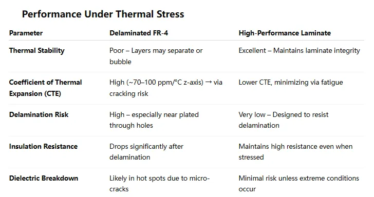
Thermal and Mechanical Stability
Dielectric materials must also handle heat and mechanical stress. During operation, PCBs can heat up, and the dielectric needs a low coefficient of thermal expansion (CTE) to avoid warping or delamination. Thermal conductivity is another factor—materials with better heat dissipation help keep components cool, extending the board’s lifespan.
Common PCB Signal Layer Materials: FR4 vs. Advanced Laminates
Now that we understand the key properties, let’s compare two broad categories of dielectric materials often used in PCB signal layers: the widely used FR4 and advanced laminates designed for high-frequency applications. Each has its strengths and trade-offs, so the choice depends on your project’s requirements.
FR4: The Standard Choice for Most Designs
FR4, which stands for Flame Retardant 4, is a glass-reinforced epoxy laminate and the most common PCB material. It’s popular for a reason—it’s cost-effective, widely available, and reliable for many applications. FR4 typically has a dielectric constant (Dk) of around 4.3 to 4.5 at 1 MHz, though this can vary slightly with frequency. Its dissipation factor (Df) is usually around 0.02, which is acceptable for low to medium-frequency designs but can lead to noticeable signal loss at higher frequencies.
FR4 works well for general-purpose electronics, such as consumer devices, power supplies, and low-speed digital circuits. However, its limitations become apparent in high-frequency or high-speed designs. The relatively high Df causes more signal attenuation, and its Dk isn’t as stable across frequencies, which can affect impedance control in applications above a few gigahertz.
Pros of FR4:
- Low cost and widely available
- Good mechanical strength and durability
- Suitable for most standard applications
Cons of FR4:
- Higher signal loss (Df around 0.02)
- Limited performance at high frequencies
- Less stable Dk with frequency and temperature changes
Advanced Laminates: Superior Performance for High-Frequency Designs
For applications requiring high-frequency signal layer materials, advanced laminates often outperform FR4. These materials are engineered with lower Dk and Df values to minimize signal loss and maintain impedance stability. Many of these laminates are based on PTFE (polytetrafluoroethylene) or ceramic-filled hydrocarbon composites, offering Dk values ranging from 2.2 to 3.5 and Df values as low as 0.001 to 0.003 at high frequencies.
These materials shine in applications like RF circuits, microwave systems, 5G technology, and high-speed digital designs (e.g., data rates above 10 Gbps). For example, in an RF design operating at 10 GHz, using a laminate with a Dk of 3.0 and Df of 0.002 can significantly reduce signal attenuation compared to FR4. The trade-off is cost—advanced laminates are often several times more expensive than FR4, and they can be harder to process during manufacturing.
Pros of Advanced Laminates:
- Low Dk and Df for minimal signal loss
- Excellent impedance stability across frequencies
- Superior thermal management for demanding environments
Cons of Advanced Laminates:
- Higher cost compared to FR4
- More complex manufacturing requirements
- Overkill for low-frequency or simple designs
FR4 vs. Advanced Laminates: Which Is Right for Your Signal Layers?
Choosing between FR4 and advanced laminates for your PCB signal layers boils down to your design’s specific needs. Let’s explore some common scenarios to help guide your decision.
Application-Based Selection
For general-purpose electronics operating below 1 GHz, FR4 is usually the best choice. Think of projects like simple microcontrollers, LED drivers, or basic power supplies. The signal speeds are low enough that FR4’s higher Df and less stable Dk won’t cause noticeable issues, and the cost savings are significant.
On the other hand, if you’re designing for high-frequency applications—such as RF antennas, satellite communications, or high-speed digital circuits—advanced laminates are worth the investment. These materials ensure cleaner signal transmission at frequencies above 5 GHz or data rates exceeding 10 Gbps. For instance, in a 5G base station PCB, a laminate with a Dk of 3.2 and Df of 0.003 can maintain signal integrity over long traces, where FR4 would fail.
Cost vs. Performance Trade-Off
Budget is always a factor in PCB design. FR4 is often a fraction of the cost of advanced materials, making it ideal for prototypes or mass-produced consumer products where margins are tight. However, if performance is non-negotiable, such as in aerospace or medical devices, the higher upfront cost of advanced laminates pays off in reliability and reduced signal loss.
Impedance and Signal Integrity
Impedance control is critical in high-speed designs. The dielectric constant directly affects the characteristic impedance of traces, which must often be maintained at specific values like 50 ohms for RF or 100 ohms for differential pairs. Advanced laminates offer tighter Dk tolerances (e.g., ±0.05) compared to FR4 (often ±0.2), making them better for precise impedance matching. If your design requires strict impedance control, especially at high frequencies, advanced materials are the safer bet.
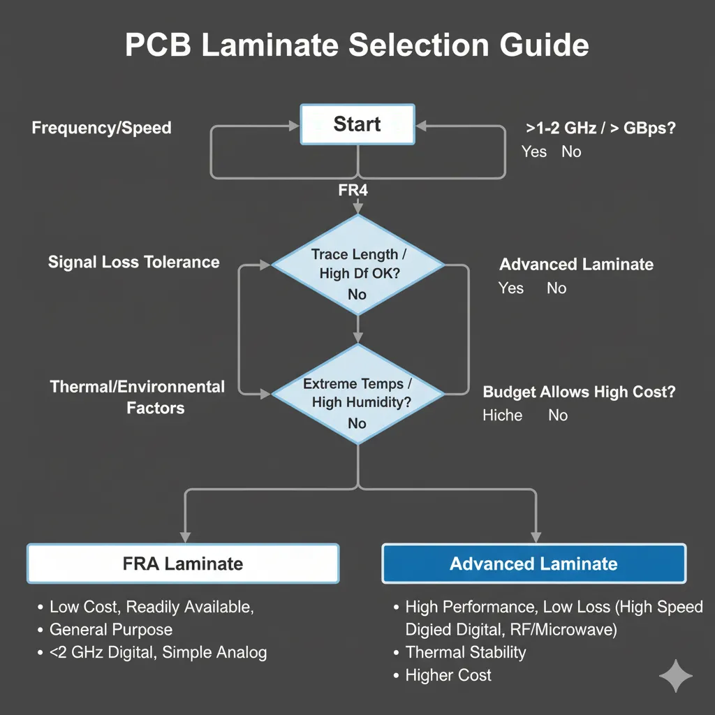
How to Choose the Right Dielectric Material for Your PCB
Selecting the right dielectric for your PCB signal layers involves a systematic approach. Follow these steps to ensure you make the best choice for your project.
1. Define Your Frequency and Speed Requirements
Start by determining the operating frequency or data rate of your design. If you’re working below 1-2 GHz or at low data rates (e.g., under 1 Gbps), FR4 is likely sufficient. For higher frequencies or speeds, consider advanced laminates with lower Dk and Df values to minimize signal loss.
2. Evaluate Signal Loss Tolerance
Calculate how much signal loss your design can tolerate. For short traces or low-frequency signals, a higher Df like 0.02 (common in FR4) may be acceptable. For long traces or high-frequency signals, aim for a Df below 0.005 to keep losses minimal.
3. Consider Thermal and Environmental Factors
Look at the operating environment of your PCB. Will it face extreme temperatures or humidity? Advanced laminates often have better thermal stability and lower CTE, preventing issues like delamination in harsh conditions. If your design operates in a controlled environment, FR4’s thermal properties may suffice.
4. Balance Cost and Performance
Finally, weigh the cost against the performance benefits. If your budget allows, investing in a high-performance dielectric can save you from costly redesigns or field failures. For less demanding projects, sticking with FR4 keeps expenses down without sacrificing quality.
Practical Tips for Working with Dielectric Materials
Once you’ve chosen a dielectric material, keep these tips in mind to optimize your design and manufacturing process:
- Collaborate with Your Manufacturer: Different materials have unique processing requirements. Work closely with your PCB fabrication team to ensure they can handle your chosen dielectric, especially if it’s an advanced laminate.
- Specify Dk and Df in Your Design Files: Clearly note the required dielectric properties in your design documentation to avoid mismatches during production. Include test frequencies if relevant (e.g., Dk at 10 GHz).
- Test for Signal Integrity: Use simulation tools to model how your chosen material affects signal propagation and impedance. This can catch potential issues before you build a prototype.
- Consider Hybrid Designs: In some cases, you can use a mix of materials in a single PCB. For example, use FR4 for power and ground layers and an advanced laminate for high-frequency signal layers to balance cost and performance.
Conclusion: Making the Right Choice for Your PCB Signal Layers
Choosing the right dielectric material for your PCB signal layers is a critical step in achieving a successful design. Whether you opt for the cost-effective and reliable FR4 or invest in advanced laminates for high-frequency signal layer materials, understanding properties like dielectric constant (Dk) and dissipation factor (Df) ensures your board meets performance expectations. By assessing your application’s frequency, signal loss tolerance, and budget, you can confidently select a material that delivers the best results.
At ALLPCB, we’re committed to helping you navigate these decisions with expert guidance and high-quality manufacturing services. Whether you’re designing for standard electronics or cutting-edge high-speed systems, we’ve got the tools and expertise to bring your vision to life. Start your next project with confidence, knowing you’ve chosen the right dielectric for your PCB.


