ALLPCB


Introduction
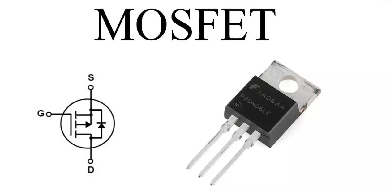
Power MOSFETs are semiconductor switching devices widely used in power management, signal processing, automotive electronics, and renewable energy systems. Switching speed is affected by internal capacitances, typically specified in datasheets as Ciss (input capacitance) and Coss (output capacitance), which originate from Cgs and Cgd between gate and source/drain. In addition to these capacitance parameters, measuring gate charge (Qgs and Qgd) is a key metric for evaluating MOSFET switching performance.
JEDEC Gate Charge Test Method
The JEDEC JESD24-2 standard describes a gate charge test method that measures MOSFET gate charge by applying a time-varying gate-to-source voltage and deriving gate–source charge (Qgs), gate–drain charge (Qgd) and total gate charge (Qg) from the resulting waveform.
Overview of Gate Charge Measurement
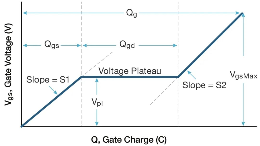
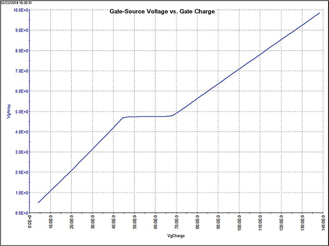
In the gate charge method, a fixed test current (Ig) is sourced into the MOSFET gate and the gate–source voltage (Vgs) is measured as a function of the injected charge. A constant bias is applied to the drain terminal. Figure 1 shows the relationship between gate voltage and gate charge for a power MOSFET.
Gate charge Q is obtained from the applied gate current and the duration (Ig·dt). Gate–source charge (Qgs) is the charge required to reach the onset of the saturation region where Vgs becomes nearly constant. According to JEDEC, the platform (Miller) voltage (Vpl) is defined as the Vgs value where dVgs/dt is minimum. The charge required to switch the device from the platform start to the end of the platform is defined as gate–drain charge (Qgd), also called the Miller charge. Total gate charge Qg is the charge from the origin to a specified maximum gate voltage VgsMax.
Measurement Waveforms
S1 is the slope of the segment from the origin to the first saturation voltage point. S2 is the slope from the last platform point to the specified maximum gate voltage VgsMax. Per JESD24-2, Qgs and Qgd are calculated using these slopes.
Using the 4200A-SCS to Measure Gate Charge
The 4200A-SCS parameter analyzer supports gate charge measurements using two source-measure units (SMUs) and a gate charge test routine included in the system. The procedure in this guide describes how to measure MOSFET gate charge with the 4200A-SCS using the JEDEC gate charge method.
Test Circuit and Operation
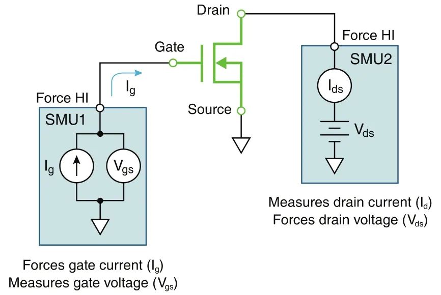
The gate charge measurement uses two SMUs. One SMU (SMU1) Force HI is connected to the MOSFET gate to apply the gate current Ig and to measure Vgs as a function of time. A second SMU (SMU2) applies a fixed voltage Vds to the drain, with a specified compliance current (Ids). The 4200-SMU has a maximum compliance of 0.1 A; the 4210-SMU has a maximum compliance of 1 A.
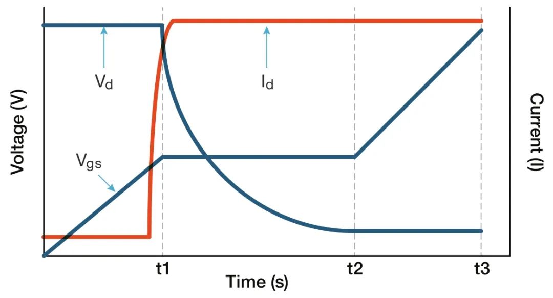
As the gate voltage rises and the transistor turns on, the drain SMU transitions from voltage-control to current-control mode when current exceeds the specified compliance. During the OFF-to-ON transition the software records transient drain current and drain voltage.
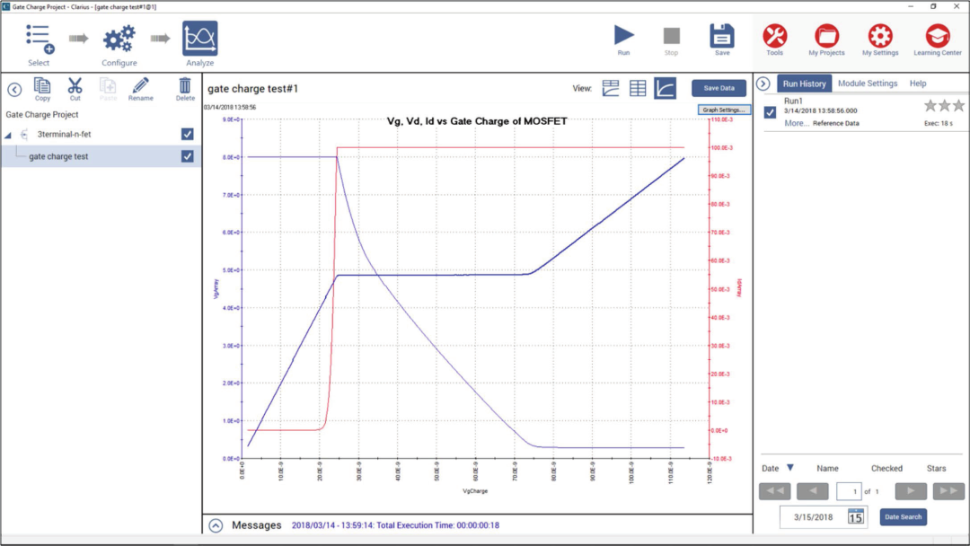
Configuring the Test in Clarius+
The Gate Charge test is available in the test library and project library; it can be added to a project from the selection pane. The test is implemented by the gate_charge user module in the GateCharge user library.
Input Parameters
Before running the test, set input parameters in the Clarius configuration pane. Input parameters vary depending on the device and the SMU models used.
Specify which SMU is connected to the gate (gate SMU) and to the drain (drain SMU). The source terminal should always be connected to GNDU or Force LO. Ig is the gate current applied by the gate SMU. Vds is the bias applied to the drain, and LimitI is the drain SMU compliance current. An offset parameter is available to compensate for offset capacitance; this is described below.
Correcting Offset Capacitance
Wiring and fixturing in the measurement system can introduce offset capacitance ranging from a few pF to several hundred pF. These parasitic capacitances can be corrected by performing an open-circuit gate_charge measurement to determine the offset capacitance, then entering that value in the software for compensation. The steps are:
- Measure offset capacitance: configure test parameters including gate current and connect the SMUs to the test fixture. For the Ceff measurement, set VgsMax as required. Before executing the test, remove the device from the fixture or lift the probe so the gate is open-circuit. Run the gate charge test with the gate open.
- Obtain offset capacitance: after the test, the measured offset capacitance appears in the worksheet Ceff column. Ceff is extracted from VgsMax, the gate current, and the timing. Because the test was run open-circuit, the test status may return codes such as -9 or -12 indicating no device measurement; this does not affect the correctness of the Ceff value. Enter this Ceff as the C offset in the configuration view.
- Enter the measured offset capacitance and run the test: in the configuration pane, enter the measured offset capacitance Ceff. The default offset is 0 F. Subsequent readings will be compensated for the offset capacitance.
Running the Test
After setting input parameters, execute the test using the Run command. While the test runs, the gate charge waveform updates in the analysis view and calculated output parameters appear in the worksheet.
Output Parameters
When the test completes, several parameters are returned in the worksheet.
Graphical Results
Gate–source voltage can be plotted as a function of gate charge, or drain current and drain voltage can be plotted as functions of time. Figure below shows a typical gate voltage waveform produced by the 4200A-SCS.
Vgs, Vds and Id can also be plotted as functions of gate charge. Following Figure shows the Clarius analysis view with all three parameters plotted versus gate charge; voltage is plotted on the Y1 axis and current on the Y2 axis.
Test Status
Each test execution returns a test status value in the worksheet first column named "gate_charge".
Summary
The 4200A-SCS parameter analyzer, using two SMUs connected to the gate and drain and the Clarius software, can derive gate charge waveforms for MOSFETs according to the JEDEC gate charge test method.