ALLPCB


When designing high-speed printed circuit boards (PCBs), one of the most important factors to consider is impedance control. Why does it matter so much? Simply put, impedance control ensures that signals travel through your PCB without distortion, maintaining signal integrity in high-speed applications like telecommunications, computing, and automotive electronics. A key element in achieving this is selecting the right PCB material for impedance control. In this blog, we’ll dive deep into how materials impact impedance, why they are critical for high-speed designs, and how to choose the best options for your project.
Whether you’re looking into high-speed PCB materials, understanding dielectric constant for PCB impedance, or designing a PCB stackup for controlled impedance, this guide will walk you through the essentials. Let’s explore the details of controlled impedance materials and their role in modern electronics design.
Why Impedance Control Matters in High-Speed PCB Design
In high-speed PCB design, signals move at incredibly fast rates, often in the range of gigahertz (GHz). At these speeds, even tiny mismatches in impedance can cause signal reflections, crosstalk, or data loss. Impedance control is the practice of designing PCB traces, layers, and materials to maintain a consistent electrical impedance, typically measured in ohms (Ω). For example, common impedance values in high-speed designs are 50Ω for single-ended traces and 100Ω for differential pairs.
Without proper impedance control, you risk signal degradation, which can lead to system failures in critical applications. This is where PCB material selection plays a pivotal role. The material’s properties directly influence how signals propagate through the board, affecting both performance and reliability.
The Role of PCB Materials in Impedance Control
PCB materials are not just a physical base for your circuit; they determine how electrical signals behave. The two primary properties of PCB materials that affect impedance are the dielectric constant (Dk) and the dissipation factor (Df). Let’s break these down:
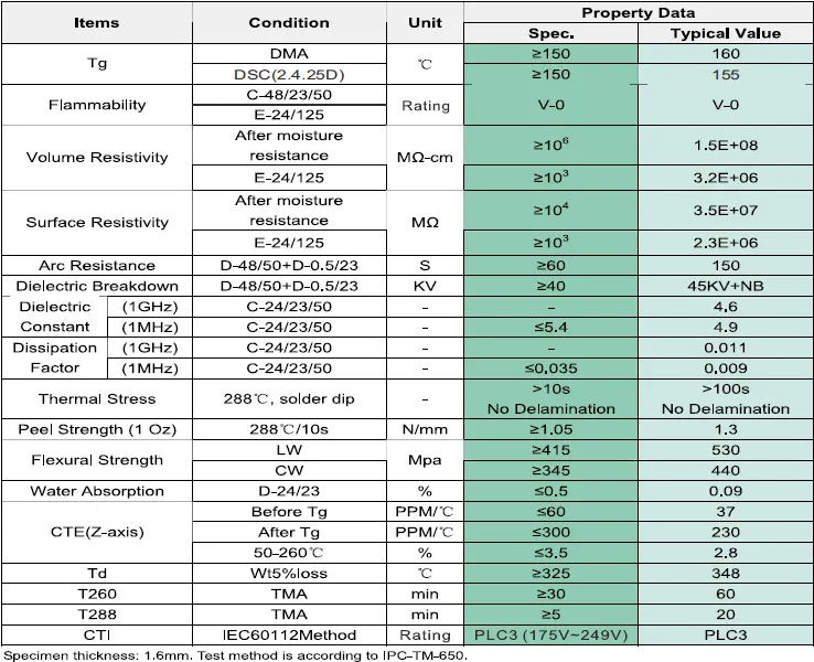
- Dielectric Constant (Dk): This value indicates how much a material can store electrical energy in an electric field. A lower Dk means faster signal propagation, which is ideal for high-speed designs. For instance, standard FR-4 material has a Dk of about 4.2-4.5, while advanced high-speed materials can have a Dk as low as 3.0 or below.
- Dissipation Factor (Df): This measures the energy loss in the material as signals pass through. A lower Df reduces signal loss, which is crucial at high frequencies. High-speed materials often have a Df of 0.002 or less, compared to FR-4’s typical Df of 0.02.
Choosing a material with the right Dk and Df is essential for maintaining controlled impedance. If the material properties vary even slightly across the board, it can lead to impedance mismatches, causing signal integrity issues.
Common High-Speed PCB Materials for Impedance Control
Not all PCB materials are suited for high-speed designs. Let’s look at some commonly used controlled impedance materials and their characteristics:
- FR-4: This is the most widely used PCB material due to its affordability and versatility. However, with a Dk of around 4.2-4.5, it’s not always ideal for very high-speed designs above 1 GHz, as it can introduce signal delays and losses.
- High-Speed Laminates: These materials are specifically engineered for high-frequency applications. They offer lower Dk values (around 3.0-3.5) and lower Df (around 0.002-0.005), making them perfect for controlled impedance in designs operating at 5 GHz or higher.
- PTFE-Based Materials: Often used in RF and microwave applications, these materials have an extremely low Dk (around 2.1-2.5) and minimal signal loss, ensuring excellent impedance control at ultra-high frequencies.
Selecting the right material depends on your design’s frequency range, budget, and performance needs. For instance, a 10 GHz design will likely require a high-speed laminate or PTFE-based material, while a 500 MHz design might work fine with enhanced FR-4.
Dielectric Constant and PCB Impedance: A Deep Dive
The dielectric constant (Dk) of a PCB material is a critical factor in determining the impedance of transmission lines on the board. Impedance is calculated using formulas that factor in the Dk, trace width, trace height, and the distance between the trace and the reference plane (usually a ground or power plane).
For a microstrip transmission line (a common configuration in PCBs), the characteristic impedance (Z?) can be approximated with the formula:
Z? = (87 / √(Dk + 1.41)) * ln(5.98 * h / (0.8 * w + t))
Where:
- h is the height of the dielectric (distance to the reference plane),
- w is the width of the trace,
- t is the thickness of the trace,
- Dk is the dielectric constant of the material.
From this formula, it’s clear that a higher Dk results in lower impedance for the same trace dimensions. This is why high-speed PCB materials with lower Dk values are often preferred—they allow for tighter control over impedance without requiring extremely narrow traces, which can be harder to manufacture.
PCB Stackup Design for Controlled Impedance
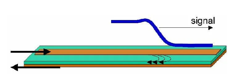
Another critical aspect of achieving controlled impedance is the PCB stackup design. The stackup refers to the arrangement of copper layers and dielectric materials in a multilayer PCB. A well-designed stackup ensures consistent impedance across all signal layers by controlling the spacing between traces and reference planes.
Here are some key considerations for PCB stackup impedance:
- Layer Symmetry: A symmetrical stackup helps maintain uniform impedance and reduces the risk of board warpage during manufacturing. For example, in an 8-layer board, place signal layers and reference planes in a balanced manner.
- Dielectric Thickness: The thickness of the dielectric between a signal layer and its reference plane directly affects impedance. Thinner dielectrics result in lower impedance, which can be useful for high-density designs but requires precise material selection.
- Reference Planes: Ensure that high-speed signal traces are routed next to a continuous ground or power plane. Gaps or splits in the reference plane can disrupt impedance and cause signal reflections.
For instance, in a 4-layer PCB stackup for a high-speed design, a common configuration is Signal-Ground-Power-Signal. This setup provides reference planes for both signal layers, ensuring stable impedance control. However, for more complex designs with 6 or more layers, additional ground planes may be needed to isolate high-speed signals and minimize crosstalk.
Factors to Consider When Selecting PCB Materials for Impedance Control
Choosing the right material for high-speed PCB design involves balancing several factors. Here’s what to keep in mind when evaluating controlled impedance materials:
- Frequency Range: Higher frequencies demand materials with lower Dk and Df to minimize signal loss. For designs above 5 GHz, consider high-speed laminates or PTFE-based materials.
- Thermal Performance: High-speed designs often generate more heat. Ensure the material can handle the operating temperature without degrading its electrical properties. Some materials have better thermal stability, with glass transition temperatures (Tg) above 170°C.
- Cost: Advanced materials with low Dk and Df are more expensive than standard FR-4. Weigh the performance benefits against your project budget.
- Manufacturability: Some materials are harder to process and may require specialized fabrication techniques. Check with your manufacturing partner to ensure compatibility with their processes.
By carefully evaluating these factors, you can select a material that meets both the technical and practical needs of your high-speed design.
Best Practices for Achieving Controlled Impedance in High-Speed Designs
Beyond material selection and stackup design, there are several best practices to ensure controlled impedance in your PCB:
- Accurate Impedance Calculations: Use impedance calculators or simulation software to predict the impedance of your traces based on material properties and stackup design. Many design tools offer built-in calculators for this purpose.
- Tight Manufacturing Tolerances: Work closely with your fabrication partner to specify tight tolerances for trace width, spacing, and dielectric thickness. Even a 10% variation in trace width can significantly affect impedance.
- Testing and Validation: After fabrication, use tools like Time Domain Reflectometry (TDR) to measure the actual impedance of your PCB traces. This helps verify that the design meets the target impedance (e.g., 50Ω or 100Ω).
- Minimize Vias: Vias can introduce impedance discontinuities in high-speed signals. If vias are necessary, use back-drilling to remove unused via stubs and reduce signal reflections.
Following these practices will help ensure that your high-speed design performs reliably under real-world conditions.
Challenges in PCB Material Selection for Impedance Control
While selecting the right material is crucial, it comes with challenges. One common issue is material consistency. Even within the same batch, some materials may exhibit slight variations in Dk or thickness, leading to impedance mismatches. To mitigate this, source materials from reputable suppliers and request detailed material datasheets with measured Dk and Df values at your operating frequency.
Another challenge is balancing cost and performance. High-speed materials can significantly increase the cost of a PCB, especially for large-scale production. In such cases, consider hybrid stackups, where high-speed layers use advanced materials while less critical layers use standard FR-4. This approach can reduce costs without compromising signal integrity.
Conclusion: Making the Right Choice for High-Speed PCB Design
In high-speed PCB design, achieving controlled impedance is non-negotiable for maintaining signal integrity and ensuring reliable performance. The choice of PCB material for impedance control is a critical factor that directly impacts how signals behave on your board. By understanding the role of dielectric constant in PCB impedance, designing an effective PCB stackup for impedance, and selecting the right high-speed PCB materials, you can optimize your design for success.
Whether you’re working on a telecommunications device operating at 10 GHz or a high-speed computing system, the principles of controlled impedance materials remain the same. Take the time to evaluate your material options, simulate your stackup design, and collaborate with your manufacturing partner to achieve the best results. With the right approach, you can build PCBs that meet the demands of even the most challenging high-speed applications.