 ALLPCB


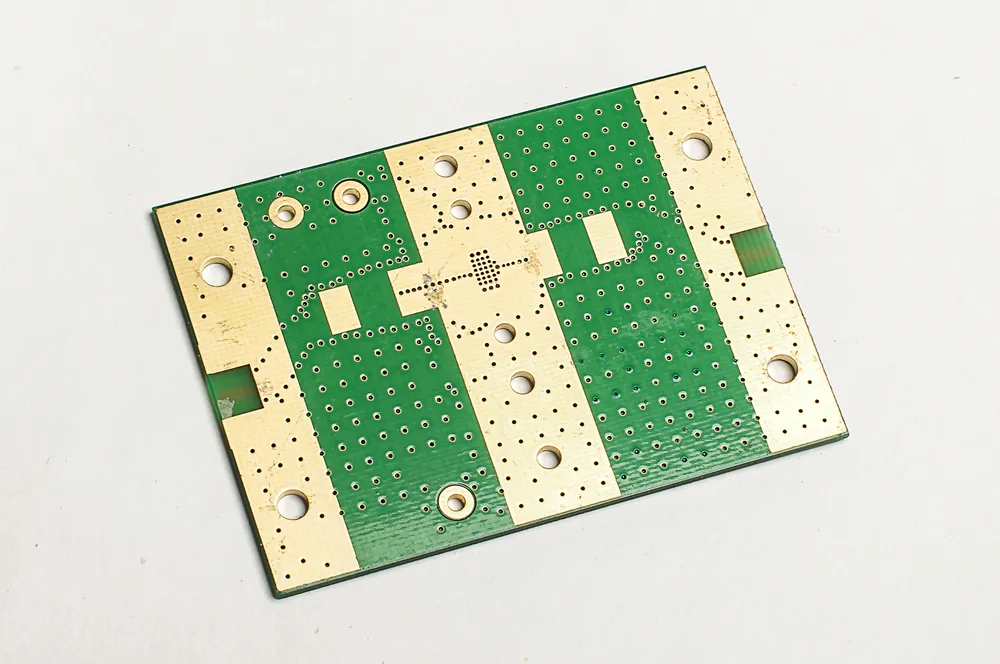
In the world of printed circuit board (PCB) design, maintaining signal integrity is crucial, especially for high-speed and high-frequency applications. Two key elements that play a significant role in this are blind via pad design and anti-pad design. But what exactly are these components, and how do they impact signal integrity in PCB design? In this comprehensive guide, we'll explore the fundamentals of blind vias and anti-pads, their importance in preserving signal quality, and PCB design best practices for vias to help engineers achieve optimal performance.
Whether you're working on a multilayer PCB for a telecommunications device or a high-speed computing system, understanding how to design blind via pads and anti-pads can make a significant difference. Let’s dive into the details to ensure your designs meet modern performance standards.
What Are Blind Vias and Why Are They Important for Signal Integrity?
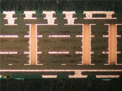
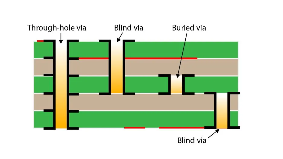
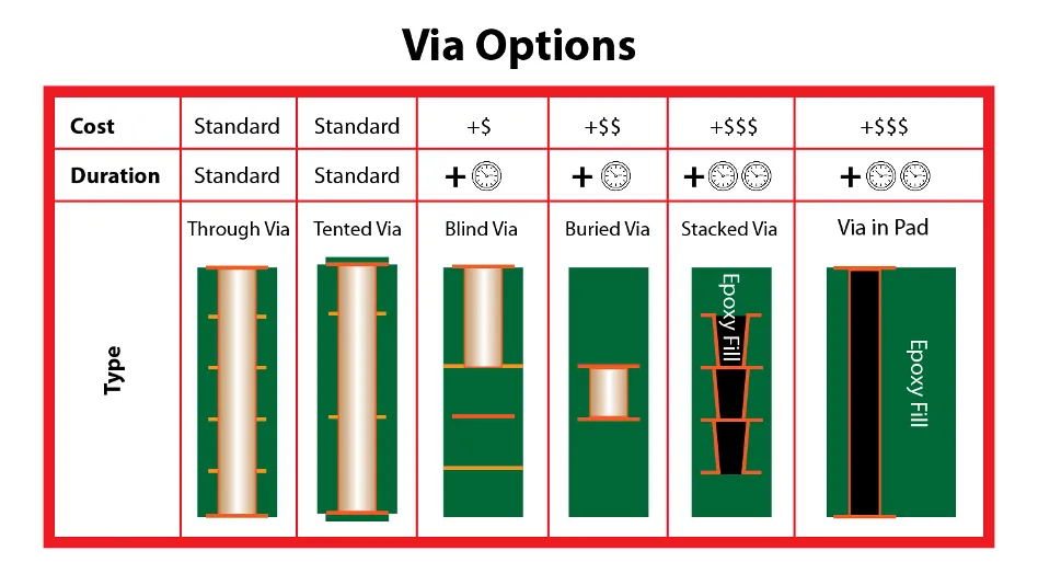
Blind vias are a type of vertical interconnect access (VIA) used in multilayer PCBs to connect an outer layer to one or more inner layers without passing through the entire board. Unlike through-hole vias, which go through all layers, blind vias are only visible on one side of the board, making them ideal for high-density interconnect (HDI) designs where space is limited.
The primary benefit of blind vias in terms of signal integrity in PCB design is their ability to reduce signal path length and minimize parasitic capacitance and inductance. In high-speed circuits, long signal paths can introduce delays and distortions. By using blind vias, signals can travel shorter distances between layers, reducing the risk of signal degradation. For example, in a 5G communication board operating at frequencies above 1 GHz, blind vias can help maintain signal clarity by limiting interference.
Blind Via Pad Design: Key Considerations
The pad design for blind vias is a critical factor in ensuring reliable connections and maintaining signal integrity. The pad is the conductive area on the PCB surface where the via connects to a trace or component. A poorly designed pad can lead to issues like signal reflection or mechanical stress during manufacturing.
1. Pad Size and Shape
The size of the pad for a blind via should be carefully calculated based on the via’s diameter and the manufacturing process. Typically, the pad diameter should be at least 1.5 times the via drill diameter to ensure proper plating and connection. For instance, if the blind via has a drill diameter of 0.2 mm, the pad should be at least 0.3 mm in diameter. A round pad shape is most common as it provides uniform stress distribution during drilling and plating.
2. Aspect Ratio
The aspect ratio, which is the ratio of via depth to diameter, is another crucial factor. For blind vias, a lower aspect ratio (ideally below 1:1) is preferred to ensure reliable plating and avoid signal loss. High aspect ratios can lead to uneven copper deposition, increasing impedance mismatches that degrade signal quality.
3. Placement and Routing
Place blind via pads strategically to avoid interference with nearby traces or components. In high-speed designs, ensure that the via is as close as possible to the signal source or destination to minimize stub effects—unused portions of the via that can act as antennas, causing reflections. Routing signals through blind vias in a controlled manner also helps maintain consistent impedance, often targeted at 50 ohms for high-frequency applications.
What Is an Anti-Pad, and How Does It Affect Signal Integrity?
An anti-pad, sometimes called a clearance pad, is a void or non-conductive area around a via on an internal plane layer of a PCB. Its purpose is to prevent unwanted electrical connections between the via and the plane, such as a ground or power plane, while controlling the impedance of the via structure. In high-speed designs, anti-pads are essential for maintaining signal integrity in PCB layouts.
Without an anti-pad, a via passing through a plane could create a short circuit or introduce excessive capacitance, disrupting the signal. By carefully designing the anti-pad, engineers can fine-tune the impedance of the via to match the trace impedance, reducing reflections and ensuring clean signal transmission. For example, in a design with a 50-ohm characteristic impedance, the anti-pad size can be adjusted to minimize deviations from this value.
Blind Via Anti-Pad Design: Best Practices
Combining blind via anti-pad design with proper planning can significantly enhance signal performance in multilayer PCBs. Here are some best practices to follow:
1. Determine the Correct Anti-Pad Size
The size of the anti-pad depends on the via diameter, the layer stack-up, and the desired impedance. As a general rule, the anti-pad diameter should be 2 to 3 times the via drill diameter. For a 0.2 mm via, an anti-pad of 0.4 to 0.6 mm is often suitable. However, simulation tools can provide more precise values by modeling the electromagnetic behavior of the via and plane interaction at specific frequencies, such as 10 GHz for high-speed data lines.
2. Consider Layer-Specific Anti-Pads
In multilayer PCBs, different internal planes may require different anti-pad sizes based on their function (e.g., ground vs. power). For blind vias that only penetrate certain layers, ensure that anti-pads are applied only to the relevant planes to avoid unnecessary capacitance or inductance.
3. Minimize Capacitive Coupling
Excessive capacitive coupling between the via and the plane can slow down signal rise times, especially in circuits operating above 1 GHz. A well-designed anti-pad reduces this coupling by increasing the distance between the via barrel and the plane. Use PCB design software to simulate and adjust the anti-pad for minimal coupling effects.
PCB Design Best Practices for Vias and Signal Integrity
Beyond specific considerations for blind via pads and anti-pads, following broader PCB design best practices for vias can further enhance signal integrity. These guidelines apply to all types of vias and are especially important in high-speed and HDI designs.
1. Use Controlled Impedance Routing
Maintain consistent impedance along the entire signal path, including through vias. For high-speed signals, a mismatch as small as 5 ohms can cause significant reflections. Use simulation tools to match the impedance of traces, vias, and pads, adjusting anti-pad sizes and via dimensions as needed.
2. Optimize Via Placement
Place vias away from sensitive analog components or high-speed digital traces to avoid crosstalk. If multiple vias are needed, stagger them to reduce electromagnetic interference (EMI). In HDI designs, using blind vias can save space and allow for tighter placement without compromising signal quality.
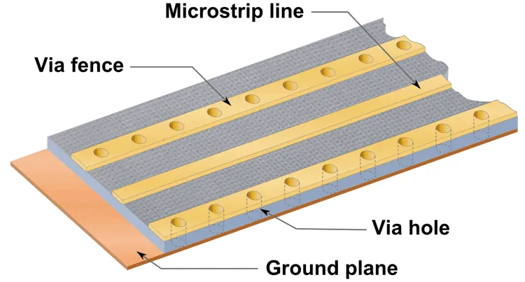
3. Incorporate Ground Planes
A solid ground plane near signal layers provides a low-impedance return path for high-frequency signals, reducing noise and EMI. Ensure that blind vias have nearby ground vias to maintain this return path, especially in designs operating at frequencies above 500 MHz.
4. Minimize Via Stubs
Via stubs, or unused portions of a via, can act as resonant structures that distort signals. For blind vias, this is less of an issue since they don’t extend through the entire board, but it’s still important to design the via depth precisely to avoid any unnecessary length.
5. Simulate and Test Designs
Before finalizing a PCB layout, use simulation software to model signal behavior through blind vias and anti-pads. Tools can predict issues like signal reflection, crosstalk, and impedance mismatches, allowing for adjustments early in the design process. Post-manufacturing testing with a time-domain reflectometer (TDR) can also verify impedance values, targeting a tolerance of ±10% for critical signals.
Common Challenges and Solutions in Blind Via and Anti-Pad Design
Designing blind vias and anti-pads for optimal signal integrity comes with challenges, especially in complex multilayer boards. Here are some common issues and how to address them:
Challenge 1: Manufacturing Limitations
Blind vias require precise drilling and plating, often using laser technology for microvias in HDI designs. If the aspect ratio is too high, plating may fail, leading to open circuits. Solution: Work closely with your PCB manufacturer to understand their capabilities and design within those limits, keeping aspect ratios below 1:1.
Challenge 2: Impedance Mismatches
Even small deviations in anti-pad size or via dimensions can cause impedance mismatches, leading to signal reflections. Solution: Use simulation tools to fine-tune anti-pad and pad dimensions, ensuring a consistent impedance (e.g., 50 ohms) across the signal path.
Challenge 3: Signal Crosstalk
In dense layouts, signals passing through nearby vias can interfere with each other, degrading performance. Solution: Space vias appropriately and use ground vias to shield high-speed signals, maintaining a separation of at least 3 times the via diameter between critical signals.
Conclusion: Enhancing Signal Integrity with Proper Design
Mastering blind via pad design and blind via anti-pad design is essential for achieving high signal integrity in PCB layouts, especially in modern high-speed and high-density applications. By carefully considering pad sizes, anti-pad dimensions, impedance control, and via placement, engineers can minimize signal loss, reduce noise, and ensure reliable performance. Following PCB design best practices for vias further enhances the quality of the final product, from controlled impedance routing to thorough simulation and testing.
At ALLPCB, we understand the importance of precision in PCB design and manufacturing. By applying the principles outlined in this guide, you can create designs that meet the stringent demands of today’s electronic applications, whether for telecommunications, computing, or consumer electronics. With the right approach, blind vias and anti-pads become powerful tools in your arsenal for maintaining signal integrity and optimizing board performance.


