 ALLPCB


Designing a radio frequency (RF) printed circuit board (PCB) is a complex task that requires precision and strategic planning, especially when it comes to component placement. Poor placement can lead to signal interference, increased noise, and degraded performance in high-frequency applications. So, how do you optimize RF PCB component placement for the best results? The key lies in following specific guidelines for orientation, spacing, and separation of analog and digital components while prioritizing high-frequency performance.
In this comprehensive guide, we’ll dive deep into RF PCB component placement guidelines, covering critical aspects such as RF PCB component orientation, RF PCB component spacing, RF PCB high-frequency component placement, and RF PCB analog and digital component separation. Whether you're an experienced engineer or just starting with RF design, this blog will provide actionable strategies to enhance your PCB layouts for optimal performance.
Why RF PCB Component Placement Matters
RF PCBs operate at high frequencies, often in the range of hundreds of megahertz (MHz) to several gigahertz (GHz). At these frequencies, even small design flaws can cause significant issues like electromagnetic interference (EMI), crosstalk, or signal loss. Component placement directly impacts signal integrity, power distribution, and thermal management. A well-thought-out placement strategy minimizes parasitic effects, reduces noise, and ensures reliable operation.
For instance, placing components too close together can lead to unwanted coupling between traces, while improper separation of analog and digital sections can introduce noise into sensitive RF signals. By adhering to proven placement practices, you can achieve a design that meets stringent performance requirements.
Suggested Image Placement: Insert an image here showing a comparison between a poorly placed RF PCB layout and an optimized one. ALT Text: "Comparison of poor vs. optimized RF PCB component placement for signal integrity."
Key Principles of RF PCB Component Placement Guidelines
Let’s break down the fundamental guidelines for placing components on an RF PCB. These principles are tailored to address the unique challenges of high-frequency designs and ensure your board performs as intended.
1. Prioritize RF PCB High-Frequency Component Placement
High-frequency components, such as RF amplifiers, oscillators, and mixers, are the heart of your design. Their placement should be your first priority to minimize signal path lengths and reduce parasitic inductance and capacitance. Here are some specific tips:
- Place RF components close to each other: Keep critical RF components near their associated circuitry to shorten trace lengths. For example, position an RF amplifier close to the antenna connector to avoid signal degradation over long traces.
- Minimize trace bends: High-frequency signals are sensitive to impedance changes caused by sharp corners. Use smooth, curved traces or 45-degree angles instead of 90-degree bends to maintain signal integrity.
- Optimize for signal flow: Arrange components in a logical order based on the signal path, from input to output. This reduces the chance of feedback loops or interference.
By focusing on RF PCB high-frequency component placement, you can significantly reduce signal loss, which is critical when dealing with frequencies above 1 GHz.
2. Master RF PCB Component Orientation
The orientation of components on an RF PCB plays a vital role in controlling EMI and maintaining signal quality. Incorrect orientation can lead to unintended coupling between components or traces. Follow these strategies for effective RF PCB component orientation:
- Align components for minimal interference: Orient components like inductors and transformers so their magnetic fields do not interfere with nearby sensitive circuits. For example, place inductors perpendicular to each other to reduce mutual coupling.
- Position connectors strategically: Place input and output connectors, such as SMA connectors for RF signals, at the edges of the board to simplify routing and reduce trace lengths.
- Rotate for thermal balance: Orient heat-generating components to distribute thermal load evenly across the board, preventing hotspots that could affect RF performance.
Proper orientation not only improves electrical performance but also aids in manufacturing and assembly by ensuring components are placed in a consistent and accessible manner.
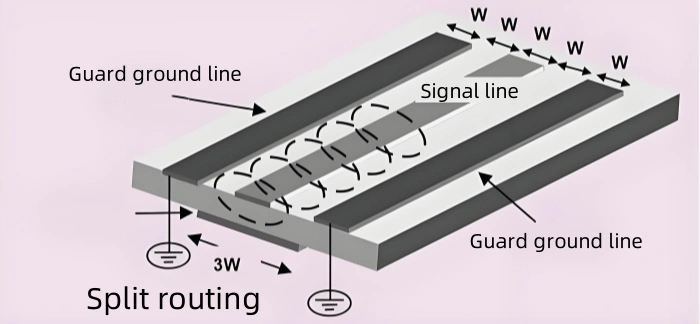
3. Maintain Proper RF PCB Component Spacing
Spacing between components is another critical factor in RF PCB design. Inadequate spacing can lead to crosstalk and EMI, while excessive spacing can increase board size and trace lengths. Here’s how to balance RF PCB component spacing:
- Follow the 3W rule for traces: Keep the spacing between adjacent signal traces at least three times the width of the trace to minimize crosstalk. For example, if a trace is 10 mils wide, maintain a spacing of at least 30 mils.
- Space high-power components: Place power amplifiers and other high-power components away from sensitive RF circuits to avoid noise coupling. A spacing of at least 100 mils is often recommended, depending on the power levels.
- Consider via spacing: Avoid placing vias too close to RF components or traces, as they can introduce unwanted capacitance. Maintain a clearance of at least 20 mils between vias and critical RF traces.
Proper spacing ensures that high-frequency signals remain isolated from noise sources, preserving the overall performance of the PCB.
4. Implement RF PCB Analog and Digital Component Separation
One of the most common challenges in RF PCB design is managing the coexistence of analog and digital components. Digital circuits often generate noise that can interfere with sensitive analog and RF signals. Effective RF PCB analog and digital component separation is essential to prevent this. Here are some best practices:
- Physically separate analog and digital sections: Place analog and digital components on different areas of the board. For instance, keep digital microcontrollers and clocks on one side and RF amplifiers on the other.
- Use separate ground planes: Split the ground plane into analog and digital sections, connecting them at a single point (often near the power supply) to avoid ground loops. This technique helps isolate noise from digital switching.
- Route signals carefully: Ensure that digital signal traces do not cross over analog or RF sections. If crossing is unavoidable, route them on different layers with a ground plane in between for shielding.
For example, in a mixed-signal PCB with an RF receiver and a digital processor, placing the processor at least 200 mils away from the RF section and using a split ground plane can reduce noise coupling by up to 20 dB at 1 GHz.
Advanced Strategies for Optimizing RF PCB Layouts
Beyond the basic guidelines, there are advanced strategies that can further enhance your RF PCB design. These techniques address specific challenges in high-frequency environments and mixed-signal applications.
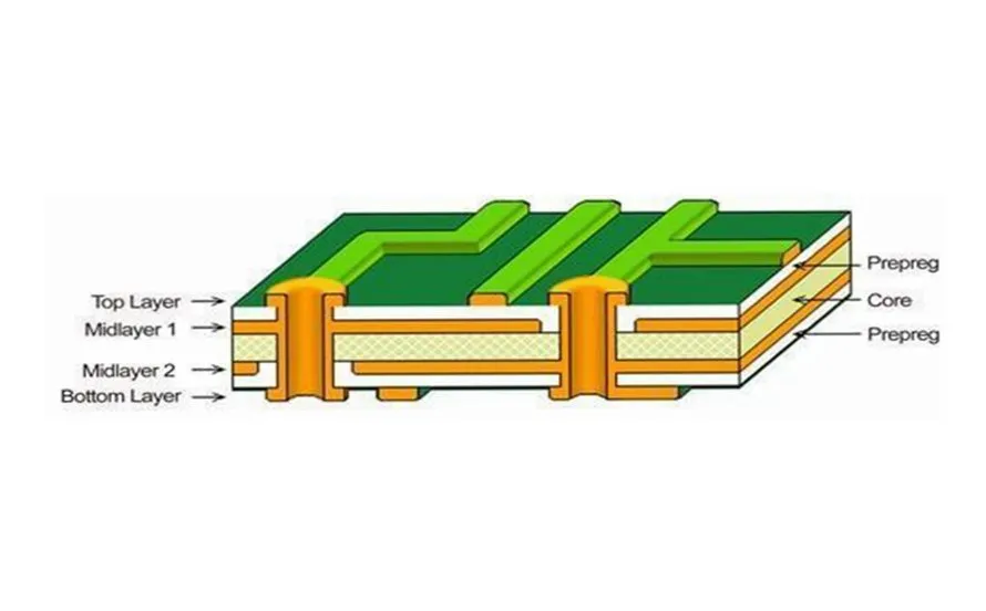
5. Use Ground Planes Effectively
A solid, continuous ground plane is a cornerstone of RF PCB design. It provides a low-impedance return path for high-frequency signals and helps shield against EMI. Consider these tips:
- Avoid breaks in the ground plane: Keep the ground plane intact under RF components and traces to prevent impedance discontinuities. Breaks can cause signal reflections, especially at frequencies above 500 MHz.
- Stitch vias for multilayer boards: In multilayer designs, use multiple ground vias to connect ground planes across layers, reducing parasitic inductance. Space vias at intervals of λ/20 (where λ is the wavelength of the highest frequency) for optimal performance.
6. Manage Thermal and Power Distribution
High-frequency components often generate significant heat, and poor thermal management can degrade performance. Additionally, power supply noise can affect RF signals. Address these issues with:
- Thermal vias: Place thermal vias under heat-generating components like power amplifiers to dissipate heat to inner layers or a heatsink.
- Decoupling capacitors: Position decoupling capacitors close to power pins of RF components to filter out noise. Use values like 0.1 μF and 1 μF in parallel to cover a wide frequency range.
Common Mistakes to Avoid in RF PCB Component Placement
Even with the best intentions, certain mistakes can undermine your RF PCB design. Be aware of these pitfalls:
- Ignoring impedance matching: Failing to match impedance between components and traces can cause signal reflections. For instance, a 50-ohm trace must connect to a 50-ohm load to avoid mismatch losses.
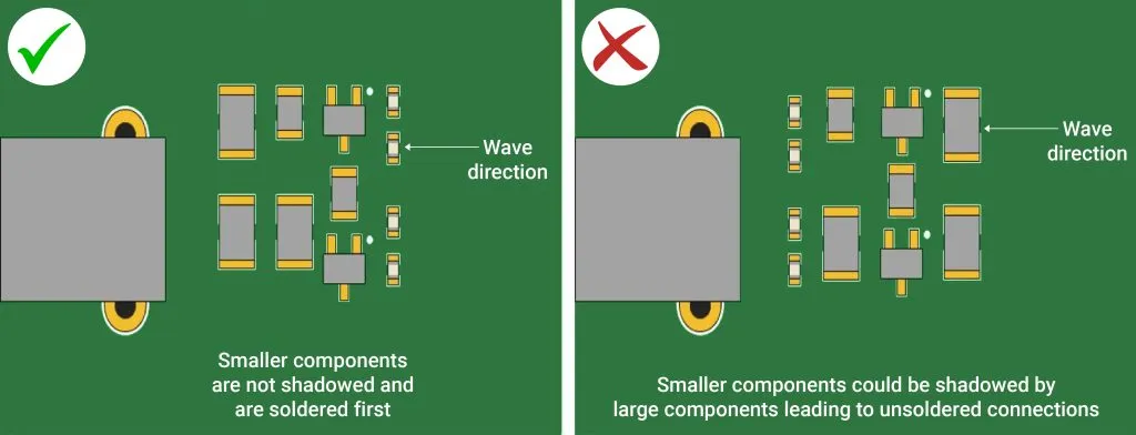
- Overcrowding components: Packing components too tightly can lead to thermal issues and EMI. Always balance density with spacing requirements.
- Neglecting shielding: Without proper shielding, external interference can disrupt RF signals. Use metal cans or grounded copper pours around sensitive areas.
Tools and Resources for RF PCB Design
Designing an RF PCB is easier with the right tools. Simulation software can help you test component placement and signal integrity before manufacturing. Look for tools that support:
- Electromagnetic simulation to predict EMI and crosstalk.
- Impedance calculators for trace design.
- Thermal analysis to identify potential hotspots.
Additionally, reference design guides and application notes from semiconductor manufacturers often provide specific placement recommendations for their RF components.
Conclusion: Building Better RF PCBs with Strategic Placement
Optimizing component placement on an RF PCB is a critical step in achieving high performance and reliability. By following RF PCB component placement guidelines, focusing on RF PCB component orientation and spacing, prioritizing high-frequency component placement, and ensuring proper analog and digital component separation, you can minimize noise, reduce EMI, and enhance signal integrity.
Remember to start with the placement of high-frequency components, use solid ground planes, and separate noisy digital circuits from sensitive analog sections. Avoid common mistakes like overcrowding or neglecting impedance matching, and leverage design tools to validate your layout. With these strategies, you’ll be well-equipped to create RF PCBs that meet the demands of modern high-frequency applications.
At ALLPCB, we’re committed to supporting engineers with resources and expertise for cutting-edge PCB designs. Apply these principles to your next project, and watch your RF designs reach new levels of performance.


