 ALLPCB


Wave soldering is a critical process in electronics manufacturing, especially for assembling printed circuit boards (PCBs) with through-hole components. For high-reliability electronics, such as those used in aerospace, medical devices, and automotive systems, optimizing wave soldering parameters is essential to ensure strong, durable solder joints and minimize defects. So, how do you achieve the best results? The key lies in fine-tuning factors like PCB wave soldering temperature, conveyor speed, flux application, preheating, and process control. In this comprehensive guide, we’ll dive deep into each of these parameters, offering actionable insights to help you achieve flawless soldering results for high-reliability applications.
Why Wave Soldering Matters for High-Reliability Electronics
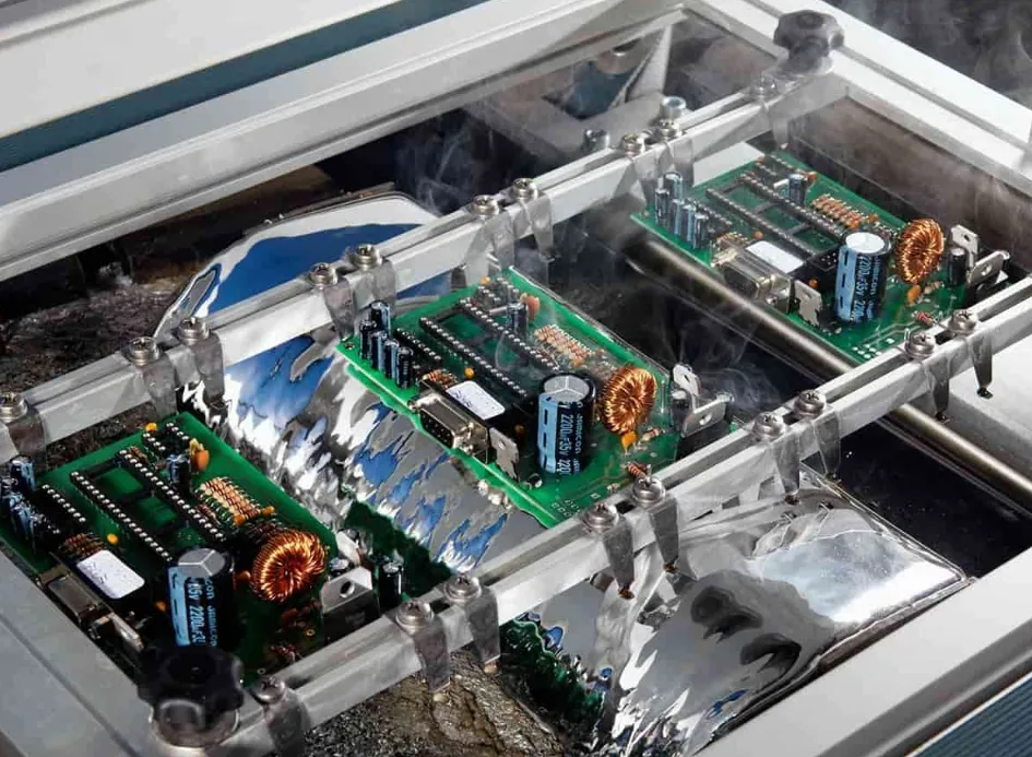
Wave soldering is a bulk soldering technique where a PCB passes over a wave of molten solder, connecting through-hole components to the board. This method is ideal for high-volume production and is often used when surface-mount technology (SMT) isn’t suitable, such as for large power devices or high-pin-count connectors. For high-reliability electronics, where failure is not an option, every solder joint must meet strict quality standards. Poorly optimized parameters can lead to defects like insufficient wetting, solder bridges, or thermal damage to components, compromising the product’s performance and longevity.
By carefully controlling the wave soldering process, manufacturers can ensure consistent, reliable connections that withstand harsh environments and extended use. Let’s break down the critical parameters and how to optimize them for the best outcomes.
1. Mastering PCB Wave Soldering Temperature
Temperature is the cornerstone of successful wave soldering. If the solder is too cool, it may not wet the component leads or PCB pads properly, leading to weak joints. If it’s too hot, it risks damaging sensitive components or causing issues like solder bridges. Striking the right balance is crucial for high-reliability electronics.
For most leaded solder alloys (like 63% tin and 37% lead), the ideal wave soldering temperature typically ranges between 250°C and 260°C (482°F to 500°F). For lead-free solders, such as SAC305 (96.5% tin, 3% silver, 0.5% copper), temperatures often need to be higher, around 260°C to 270°C (500°F to 518°F), due to their higher melting points. However, always refer to the specific alloy’s datasheet for precise recommendations.
Beyond the solder pot temperature, the thermal profile of the entire process matters. The PCB should not experience sudden temperature spikes, as thermal shock can crack components or delaminate the board. Monitoring and maintaining a stable temperature in the solder wave ensures uniform heating and consistent joint quality.
Tip for Optimization: Use a thermal profiling tool to measure the temperature across different zones of the PCB during soldering. Adjust the solder pot temperature if you notice cold spots or overheating. For high-reliability applications, aim for a tolerance of ±5°C to avoid variability.
2. Setting the Right PCB Wave Soldering Conveyor Speed
The conveyor speed determines how long the PCB is exposed to the solder wave. Too fast, and the solder may not have enough time to wet the leads and pads, resulting in incomplete joints. Too slow, and excessive heat exposure can damage components or cause solder bridges. For high-reliability electronics, precision in conveyor speed is non-negotiable.
A typical conveyor speed for wave soldering ranges from 1.0 to 1.5 meters per minute (3.3 to 4.9 feet per minute), but this varies based on the PCB design, component density, and solder type. For complex boards with high thermal mass or densely packed components, a slower speed (around 0.8 to 1.2 meters per minute) may be necessary to ensure adequate heat transfer. Conversely, for simpler designs, a slightly faster speed can improve throughput without sacrificing quality.
Tip for Optimization: Conduct trial runs with different speeds to find the sweet spot for your specific PCB assembly. Monitor the contact time with the solder wave—ideally, it should be between 2 to 4 seconds for most designs. Use a stopwatch or built-in machine settings to measure and adjust accordingly.
3. Perfecting PCB Wave Soldering Flux Application
Flux plays a vital role in wave soldering by cleaning the surfaces of the PCB and component leads, removing oxides, and promoting solder wetting. For high-reliability electronics, the right flux application can mean the difference between a robust solder joint and a failure-prone connection.
There are two common methods for applying flux: spray and foam. Spray fluxing offers precise control over the amount and distribution, making it ideal for complex boards. Foam fluxing, on the other hand, is simpler and often used for less demanding applications. The type of flux—whether rosin-based, water-soluble, or no-clean—also impacts the process. For high-reliability electronics, no-clean fluxes are often preferred to avoid residue that could lead to corrosion over time, though thorough cleaning is still recommended in critical applications.
Tip for Optimization: Ensure uniform flux coverage by regularly checking the fluxer settings. Too little flux can lead to poor wetting, while too much can cause residue buildup or solder balling. Aim for a thin, even layer—typically 0.5 to 1.0 grams per square foot of PCB area. Additionally, store flux in a controlled environment to prevent degradation, and replace it as per the manufacturer’s shelf-life guidelines.
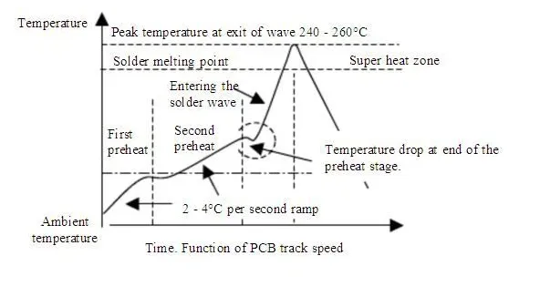
4. Importance of PCB Wave Soldering Preheating
Preheating is a critical step that prepares the PCB and components for the thermal shock of the solder wave. Without proper preheating, the sudden temperature change can cause component damage, board warpage, or poor solder joint formation. For high-reliability electronics, preheating is even more crucial to ensure consistent results and protect sensitive parts.
The preheat temperature typically ranges from 100°C to 150°C (212°F to 302°F), depending on the board’s material and thickness, as well as the type of components. For standard FR-4 boards, a preheat temperature of 120°C to 130°C is often sufficient. The duration of preheating should allow the PCB to reach a uniform temperature, usually taking 1 to 3 minutes, based on the conveyor speed and preheat zone length.
Tip for Optimization: Use infrared or convection preheaters for even heat distribution. Monitor the PCB’s top and bottom sides with a thermal probe to ensure there’s no significant temperature gradient (aim for less than 10°C difference). Adjust the preheat settings if you notice issues like insufficient solder penetration or thermal stress cracks.
5. Implementing PCB Wave Soldering Process Control
Process control ties all the parameters together, ensuring consistency and repeatability—key factors for high-reliability electronics. Without strict oversight, even minor variations in temperature, speed, or flux can lead to defects that compromise the final product.
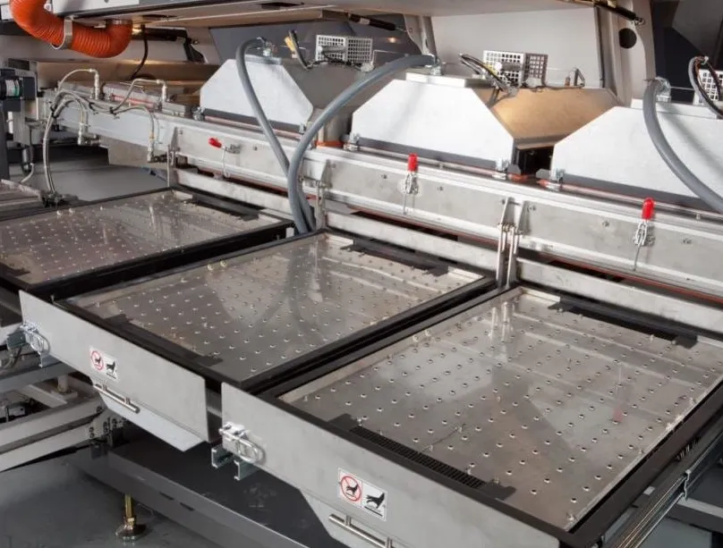
Effective process control starts with regular machine maintenance. Check solder levels daily, clean the solder pot weekly to remove dross (oxide buildup), and inspect the conveyor system for smooth operation. Use statistical process control (SPC) tools to track key metrics like solder joint defect rates, aiming for less than 1% defect per million opportunities (DPMO) in critical applications.
Additionally, implement automated monitoring systems if possible. Modern wave soldering machines often come with sensors that alert operators to deviations in temperature or conveyor speed. For high-reliability production, consider investing in nitrogen inerting systems to reduce oxidation during soldering, which can improve joint quality and reduce dross formation by up to 50%.
Tip for Optimization: Develop a detailed process checklist for every production run. Include steps like verifying solder alloy composition (e.g., tin-lead ratio), testing flux activity, and calibrating machine settings. Conduct post-soldering inspections using X-ray or automated optical inspection (AOI) to catch defects early, ensuring compliance with standards like IPC-A-610 for electronics assembly.
Common Challenges and Solutions in Wave Soldering
Even with optimized parameters, wave soldering can present challenges, especially for high-reliability electronics. Here are a few common issues and how to address them:
- Insufficient Wetting: Often caused by low solder temperature or inadequate flux. Increase the solder pot temperature by 5°C increments or adjust flux application for better coverage.
- Solder Bridges: Typically due to excessive solder or slow conveyor speed. Reduce wave height or increase speed slightly to minimize solder contact time.
- Thermal Damage: Occurs when preheat or solder temperatures are too high. Lower the settings and ensure proper thermal profiling to protect components.
For high-reliability applications, it’s also wise to conduct reliability testing, such as thermal cycling (e.g., -40°C to 85°C for 1000 cycles) and vibration testing, to validate solder joint durability under real-world conditions.
Benefits of Optimized Wave Soldering for High-Reliability Electronics
When wave soldering parameters are fine-tuned, the benefits are clear. You achieve consistent, high-quality solder joints that meet stringent industry standards. Defect rates drop, reducing rework costs and improving production efficiency. Most importantly, the reliability of the final product increases, ensuring it performs flawlessly in critical applications like medical equipment or automotive control systems.
Optimized processes also extend the lifespan of your manufacturing equipment. For instance, maintaining clean solder pots and stable temperatures reduces wear on the machine, cutting down on maintenance expenses over time.
Conclusion: Achieving Excellence in Wave Soldering
Optimizing PCB wave soldering temperature, conveyor speed, flux application, preheating, and process control is the foundation of producing high-reliability electronics. Each parameter plays a unique role in ensuring strong, defect-free solder joints that can withstand the demands of critical applications. By carefully adjusting and monitoring these factors—using precise measurements, thermal profiling, and strict process oversight—you can elevate your PCB assembly process to new heights of quality and consistency.
Whether you’re manufacturing for aerospace, medical, or industrial sectors, mastering wave soldering is a game-changer. Take the time to test and refine your settings, invest in proper equipment maintenance, and stay updated on best practices. With these steps, you’ll not only meet but exceed the expectations for high-reliability electronics, delivering products that stand the test of time.


