ALLPCB


onsemi AF013x Hyperlux ID 1.2MP indirect time-of-flight (iToF) sensor is a 3D imaging array sensor for fast-moving objects. The sensor uses a 1/3.2" optical format and a back-side illuminated (BSI) CMOS global shutter for depth and imaging. The onsemi AF013x iToF image sensors provide on-chip dual laser driver control, modulation frequencies up to 200 MHz, and laser eye-safety threshold monitoring. The AF0130 version includes a stacked depth-processing ASIC beneath the pixel area to compute depth, confidence, and intensity maps at high speed from laser-modulated exposures. The AF0131 is intended for off-chip depth computation. These sensors are suitable for factory automation, computing, drones, robotics, metrology, machine vision, biometrics, retail and logistics, and 3D modeling.
Features
- 1.2 MP CMOS smart iToF sensor using advanced 3.5 μm stacked BSI pixel technology
- Excellent low-light and ambient light performance
- Enhanced NIR response at 850 nm and 940 nm (QE > 40%)
- Dual-laser (frequency) operation to extend depth range at VGA resolution and reduce ambiguity
- Low-voltage differential signal (LVDS) drivers for modulation control of two lasers, up to 200 MHz
- Two-wire or four-wire serial interface for register access
- 2 Gbps/channel, two-lane MIPI CSI-2 D-PHY data interface
- Laser eye-safety monitoring
- Automatic exposure control (AEC)
- Pixel identification and correction (PDI and PDC)
- Hardware trigger control
- Multi-camera and interference mitigation
- Reduced motion artifacts due to separation between integration and readout
- Three output modes:
- RAW
- Data compression (DR)
- Integrated depth processing (DP)
- Phase and pulse (hybrid) modulation support
- Simultaneous output of depth, confidence, and grayscale
- Horizontal and vertical mirror, windowing, and pixel binning
- Context state machine with 64 programmable contexts
- Intelligent on-chip mean and histogram statistics
- On-chip temperature sensor
- Lead-free device compliant with RoHS
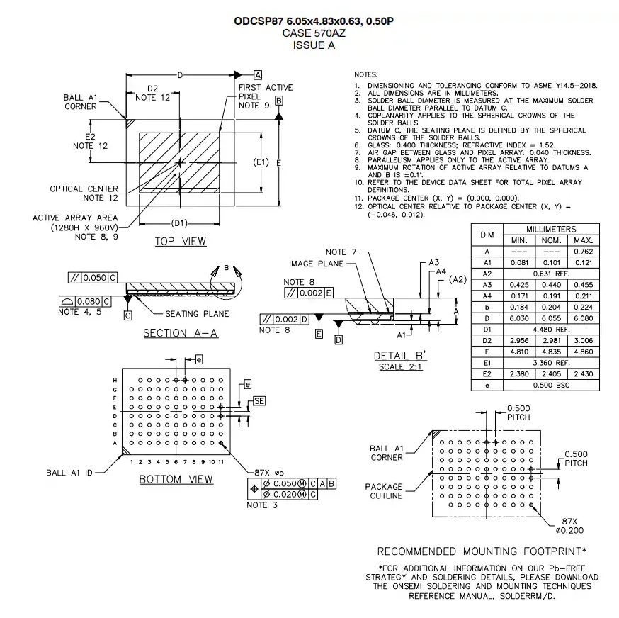
Dimensions
onsemi AF013x Hyperlux 1.2MP iToF sensor technical guide
1. Product overview
The AF0130 and AF0131 are onsemi 1.2 MP smart iToF sensors using a 1/3.2" optical format and BSI CMOS global shutter technology, designed for depth sensing and imaging. Both sensors integrate dual laser driver control and modulation capability (up to 200 MHz) and include laser eye-safety monitoring.
- AF0130: Stacked depth-processing ASIC beneath the pixel area, capable of real-time depth, confidence, and intensity map output.
- AF0131: No on-chip depth processing; intended for solutions that perform depth computation off-chip.
2. Key specifications
| Parameter | Typical value |
|---|---|
| Optical format | 1/3.2" (diagonal 5.60 mm, 4:3 aspect ratio) |
| Effective pixels | 1280 × 960 (1.2 MP) |
| Pixel size and chief ray angle | 3.5 μm, 30° CRA |
| Shutter type | BSI global shutter |
| Interface | MIPI CSI-2 (2 lanes, 2 Gbps/lane), host two-wire/four-wire laser driver, three-wire laser modulation LVDS |
| ADC resolution | 10–11 bits |
| Frame rate (mode 2.2) | Up to 60 fps @ 1.2 MP, 100 fps @ VGA |
| Power consumption | 400 mW (mode 2.2 @ 30 fps); 600 mW (mode 3.2 @ 30 fps) |
| Operating temperature | -30°C to +85°C (optimal performance: 0°C to +60°C) |
3. Key technical features
- Stacked BSI pixel technology
3.5 μm pixels with back-side illumination increase quantum efficiency in the near-infrared bands (850/940 nm, QE > 40%) and improve low-light and ambient-light performance. - Dual laser frequency operation
Supports dual-laser modulation up to 200 MHz. Frequency-division multiplexing extends measurement range at VGA resolution and reduces multi-device interference. - Multiple output modes
- RAW mode: raw data output
- Data compression (DR): reduces bandwidth requirements
- Depth processing (DP): AF0130 only, outputs depth maps, confidence, and grayscale directly
- Smart control features
- Automatic exposure control (AEC)
- Pixel identification and correction (PDI & PDC)
- 64 programmable context state machine for adaptive scene switching
4. Applications
- Machine vision: high-precision 3D modeling and object recognition
- Drones and robots: obstacle avoidance and environment perception
- Augmented/virtual reality: gesture tracking and spatial localization
- Smart logistics and security: personnel monitoring and access control
5. Design considerations and recommendations
- Power management
Power increases with exposure time and modulation frequency. Optimize operating modes in battery-sensitive applications. - Thermal design
Package thermal resistance θJA is 32.0°C/W. Implement module-level thermal management to control junction temperature and ensure stable operation in high-temperature environments. - Signal integrity
LVDS modulation interface and MIPI high-speed signals require controlled impedance routing to avoid timing distortion.
6. Selection and development support
- Model differences: AF0130 includes on-chip depth processing; AF0131 relies on external depth computation.
- Evaluation tools: evaluation kit includes AF0130 sensor headboard with lens, laser headboard, and FPGA demo board to accelerate prototyping.
- Packaging options: 6.06 mm × 4.84 mm ball-grid CSP or bare die to meet different integration density requirements.