ALLPCB


Introduction
MOSFETs can be confusing at first. Textbooks often present long, formal definitions and classifications that prioritize rigor over accessibility, which makes it hard to see practical uses. This article drops the academic framing and explains the most common and easy-to-use type: the enhancement-mode NMOS, referred to here as NMOS. Once you understand how to use an NMOS in practice, the textbook material will make more sense.
NMOS Usage
Consider a simple manual switch that controls a lamp (Figure 1). We can replace that switch with an NMOS so a microcontroller or Arduino can turn the lamp on and off.
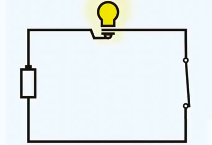
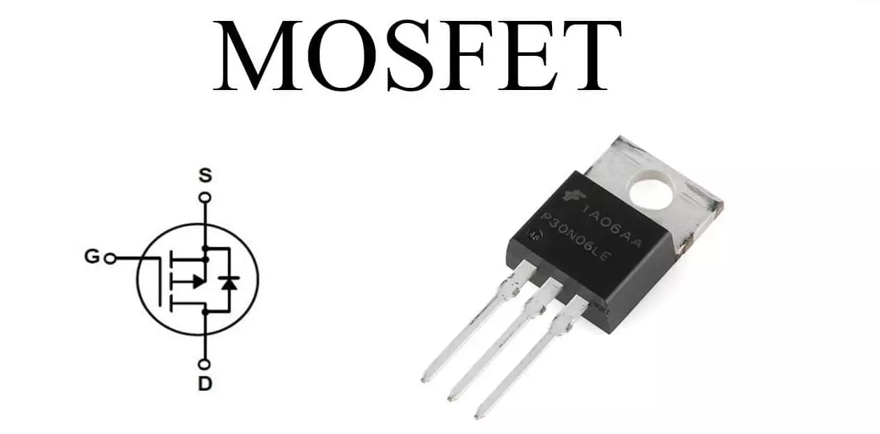
To match typical engineering practice, we redraw the circuit as in Figure 2, showing the NMOS with its three terminals: GATE, DRAIN and SOURCE, commonly abbreviated G, D, S.
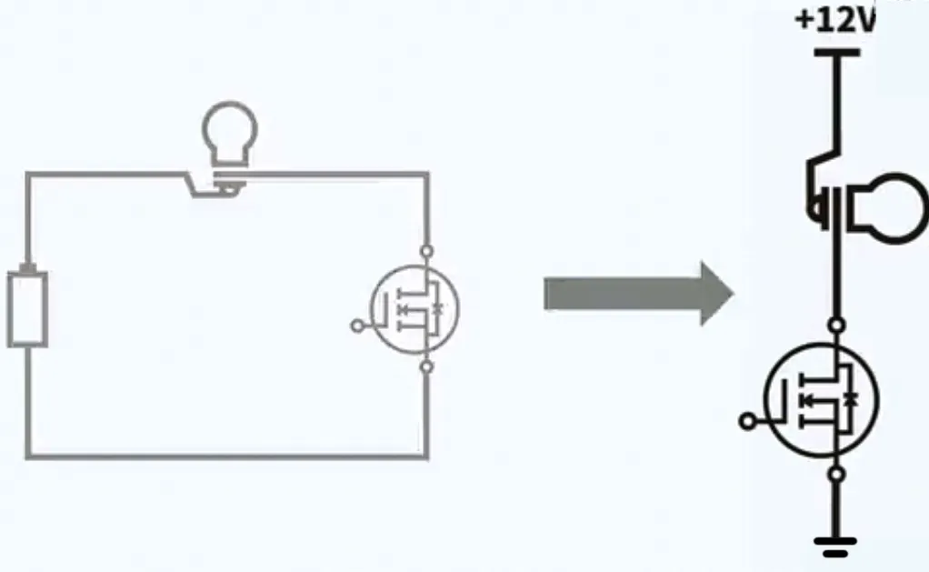
Connect a microcontroller IO pin to the NMOS gate and provide supply power. When the IO outputs a high level, the NMOS behaves like a closed switch and the lamp turns on. When the IO outputs a low level, the NMOS behaves like an open switch and the lamp turns off.
Switching the gate repeatedly makes the lamp blink. If you switch faster than the persistence of human vision, the blinking becomes imperceptible and the perceived brightness can be adjusted by changing the duty cycle. This is PWM dimming, the classic use of an NMOS: it lets a microcontroller IO control a power device. The lamp can be substituted by other loads such as pumps, motors, or solenoids.
How to Choose an NMOS
After understanding NMOS usage, the next step is selecting a suitable NMOS. For beginners, four parameters are most important: package, Vgs(th), Rds(on), and Cgs.
Package refers to the physical package and size. Larger packages generally support higher current.
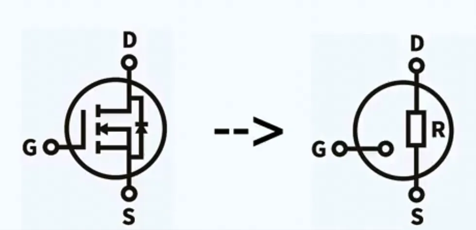
NMOS can be modeled as a voltage-controlled resistor: the gate-to-source voltage (Vgs) controls the drain-to-source resistance. The resistance varies nonlinearly with Vgs. When Vgs is below a certain threshold, the resistance is effectively infinite; above that threshold it approaches a low value. That threshold is Vgs(th), the gate-to-source voltage at which the device begins to turn on. Vgs(th) is a characteristic listed in the device datasheet.
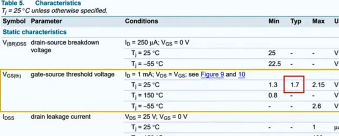
Vgs(th) must be lower than the controller's high-level output voltage for the NMOS to switch on reliably. For example, if your high level is 5 V, choosing an NMOS with Vgs(th) around 3 V is reasonable. If Vgs(th) is too low, the device may switch on due to interference; if too high, it may not fully turn on.
Rds(on) is the drain-to-source resistance when the NMOS is fully on. The smaller this resistance, the less voltage drop and the lower the power dissipation. Rds(on) is listed in the datasheet. In general, lower Rds(on) is better, but such devices tend to be larger and more expensive, so choose appropriately for the application.
Cgs is the parasitic capacitance between gate and source. All NMOS devices have this capacitance due to fabrication. Cgs affects switching speed because the gate drive must charge this capacitance before the gate-to-source voltage reaches its intended value. Although Cgs is usually small and often unnoticed, at high PWM frequencies the gate charge time can distort the waveform. If the PWM period approaches the gate charge time, the switching waveform will be distorted. Typically, Cgs and Rds(on) trade off: devices with very low Rds(on) tend to have larger gate capacitance. Balance these parameters for your design.
These are the basic NMOS concepts you should know when getting started.