ALLPCB


In the world of electronics manufacturing, lead-free assembly has become the standard due to environmental and health regulations like RoHS (Restriction of Hazardous Substances). If you're looking to master lead-free PCB design and assembly, you're in the right place. This guide will walk you through essential aspects such as lead-free PCB design rules, component selection, high-temperature materials, solder paste application, and reflow profiling. Whether you're an engineer or a designer, you'll find actionable insights to ensure your projects meet compliance and performance standards.
Let’s dive into the details of creating reliable, high-quality lead-free printed circuit boards (PCBs) with a step-by-step approach tailored for success.
Why Lead-Free PCB Assembly Matters
Lead-free assembly isn't just a trend; it's a necessity driven by global regulations aimed at reducing toxic substances in electronics. Traditional lead-based solders have been phased out in many regions due to their environmental and health risks. Switching to lead-free alternatives, like tin-silver-copper (SAC) alloys, ensures compliance with laws and promotes safer manufacturing practices.
Beyond compliance, lead-free assembly offers benefits like improved long-term reliability under certain conditions and compatibility with modern components designed for higher temperatures. However, it also introduces challenges, such as higher reflow temperatures (often 30°C above leaded solder profiles, reaching up to 260°C) and potential issues with thermal stress on components and materials. Understanding these factors is the first step to mastering the process.
Lead-Free PCB Design Rules: Building a Strong Foundation
Designing a PCB for lead-free assembly requires careful planning to handle the unique demands of the process. Here are some critical lead-free PCB design rules to follow:
- Pad and Trace Sizing: Lead-free solders, like SAC305 (a common alloy with 3% silver, 0.5% copper, and the rest tin), have different wetting characteristics compared to leaded solders. To ensure proper solder joint formation, increase pad sizes by about 10-15% to accommodate reduced flow. Traces should also be slightly wider to handle potential thermal stress during reflow.
- Thermal Relief Pads: High reflow temperatures can cause uneven heating. Use thermal relief pads for components connected to large ground planes to prevent heat dissipation issues, ensuring consistent soldering across the board.
- Component Spacing: Allow for more spacing between components (at least 0.3 mm extra compared to leaded designs) to avoid bridging due to the less fluid nature of lead-free solder.
- Via Design: Avoid placing vias too close to solder pads, as lead-free soldering can lead to voiding or insufficient fill. A minimum clearance of 0.5 mm is recommended between vias and pads.
By adhering to these design rules, you create a PCB layout that minimizes defects and ensures reliability during lead-free assembly.
Lead-Free Component Selection Guide: Choosing the Right Parts
Selecting components for lead-free assembly is a crucial step that impacts both performance and compliance. Here's a practical lead-free component selection guide to help you make informed choices:
- Check RoHS Compliance: Ensure all components are certified as RoHS-compliant. Look for documentation or markings indicating lead-free status to avoid compatibility issues during assembly.
- Temperature Ratings: Lead-free soldering requires higher reflow temperatures (typically 240-260°C). Choose components rated for at least 260°C to withstand peak temperatures without damage. For example, capacitors and resistors should specify a maximum temperature tolerance in their datasheets.
- Lead Finish Compatibility: Opt for components with lead-free finishes like pure tin, nickel-palladium-gold (NiPdAu), or silver. Avoid older lead-based finishes that can contaminate the solder joint and compromise reliability.
- Moisture Sensitivity Level (MSL): Lead-free processes can exacerbate moisture-related issues like popcorning in components. Select parts with lower MSL ratings or ensure proper storage and handling to prevent damage during reflow.
Paying attention to these factors during component selection reduces the risk of failures and ensures a smooth assembly process.
High-Temperature PCB Materials: Ensuring Durability
The shift to lead-free assembly means dealing with higher processing temperatures, which puts additional stress on PCB materials. Choosing the right high-temperature PCB materials is essential for maintaining structural integrity and performance. Here’s what to consider:
- Laminate Selection: Use laminates with a high glass transition temperature (Tg), ideally above 170°C, to handle the thermal demands of lead-free soldering. Materials like FR-4 with enhanced Tg or polyimide are excellent choices for demanding applications.
- Thermal Decomposition Temperature (Td): Select materials with a Td above 340°C to prevent degradation during multiple reflow cycles. This ensures the PCB remains stable even after rework or repairs.
- Coefficient of Thermal Expansion (CTE): A lower CTE (around 12-16 ppm/°C) helps minimize warping and stress on solder joints caused by temperature fluctuations during reflow.
- Surface Finishes: Opt for lead-free compatible finishes like immersion silver, immersion tin, or ENIG (Electroless Nickel Immersion Gold). These finishes provide good solderability and resist oxidation at high temperatures.
Using high-temperature materials tailored for lead-free processes prevents issues like delamination, cracking, or solder joint failure, ensuring your PCB withstands the rigors of assembly.
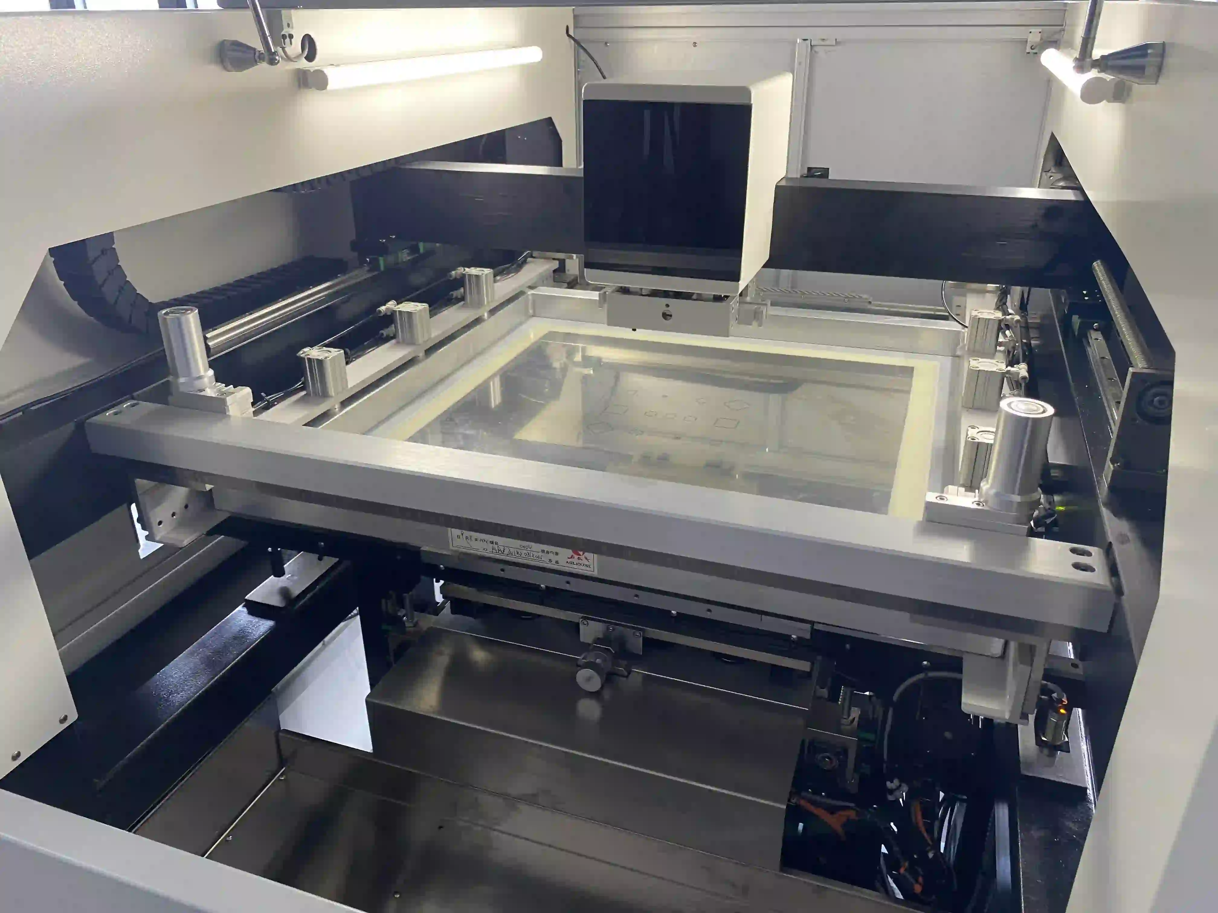
Lead-Free Solder Paste Application: Getting It Right
Applying lead-free solder paste correctly is a critical step in achieving reliable solder joints. Unlike traditional solders, lead-free pastes have different viscosities and flow characteristics. Follow these tips for effective lead-free solder paste application:
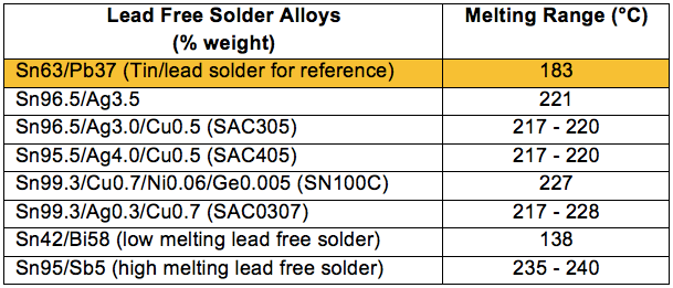
- Choose the Right Alloy: SAC305 is the most widely used lead-free solder paste due to its balanced properties, offering good wetting and mechanical strength. It typically consists of 96.5% tin, 3% silver, and 0.5% copper.
- Stencil Design: Use a stencil thickness of 0.1-0.15 mm for fine-pitch components to control the amount of paste deposited. Ensure aperture sizes are slightly reduced (by about 10%) compared to leaded designs to prevent excess paste and bridging.
- Application Precision: Use automated stencil printers for consistent paste application. Maintain a printing speed of 20-50 mm/s and a pressure of 0.1-0.3 kg/cm to avoid smearing or insufficient paste.
- Storage and Handling: Store solder paste at 2-10°C to maintain its shelf life (typically 6 months). Allow it to reach room temperature (about 25°C) for 4-6 hours before use to prevent condensation and ensure proper viscosity.
Proper application of lead-free solder paste sets the stage for a successful reflow process, minimizing defects like voids or insufficient joints.
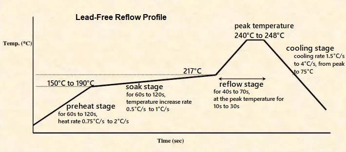
Lead-Free Reflow Profiling: Optimizing the Process
Reflow profiling is the heart of lead-free assembly, determining the quality of solder joints. Lead-free solders require higher temperatures and precise control to avoid damaging components or creating defects. Here’s how to optimize lead-free reflow profiling:
- Preheat Zone: Gradually heat the board to 150-180°C over 60-90 seconds at a rate of 1-3°C per second. This minimizes thermal shock and activates the flux in the solder paste to clean surfaces.
- Soak Zone: Maintain a temperature of 180-200°C for 60-120 seconds to ensure uniform heating across the board and evaporate any remaining solvents in the paste.
- Reflow Zone: Ramp up to a peak temperature of 240-260°C for 20-40 seconds. The time above liquidus (TAL) for SAC305, which melts at 217°C, should be 30-60 seconds to ensure proper wetting and joint formation.
- Cooling Zone: Cool the board at a rate of 2-4°C per second to below 150°C. Rapid cooling can cause thermal stress, while slow cooling may lead to grain growth in solder joints, reducing strength.
Monitoring the reflow profile with thermocouples attached to critical areas of the PCB ensures consistency. Adjust the profile based on the board’s thermal mass and component specifications to prevent issues like tombstoning or voiding.
Common Challenges in Lead-Free Assembly and How to Overcome Them
While lead-free assembly offers many advantages, it also presents unique challenges. Here are some common issues and solutions:
- Higher Thermal Stress: The elevated temperatures can stress components and boards. Mitigate this by selecting high-temperature materials and components, as discussed earlier, and optimizing reflow profiles for minimal peak duration.
- Poor Wetting: Lead-free solders wet less effectively than leaded ones. Use compatible surface finishes and ensure proper flux activity by adhering to recommended preheat and soak times.
- Tin Whiskers: Pure tin finishes on components can develop whiskers over time, risking short circuits. Choose finishes with additives or alternative coatings like NiPdAu to reduce this risk.
- Solder Joint Reliability: Lead-free joints may be more brittle. Enhance reliability by controlling cooling rates and using underfill for high-stress components like BGAs.
Addressing these challenges proactively ensures your lead-free PCBs perform reliably in real-world applications.
Conclusion: Achieving Success with Lead-Free PCB Assembly
Mastering lead-free assembly is a vital skill in today’s electronics industry. By following lead-free PCB design rules, selecting compatible components, using high-temperature materials, applying solder paste with precision, and optimizing reflow profiling, you can create PCBs that meet regulatory standards and deliver exceptional performance. Each step, from design to final soldering, plays a critical role in the success of your project.
Armed with this comprehensive guide, you’re ready to tackle the complexities of lead-free assembly with confidence. Implement these best practices in your next project to ensure compliance, reliability, and quality in every board you design and build.