ALLPCB


Low-power techniques in IC design
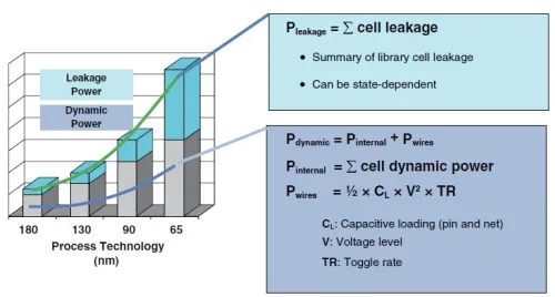
Low-power techniques in IC design are used to optimize power management and improve energy efficiency to achieve lower power consumption. The following are common low-power techniques applied in IC design:
- Power management techniques: Using multi-voltage domain design, dynamic voltage scaling, and fast power switching to provide flexible power delivery to different modules, reducing overall power consumption.
- Clock management techniques: Applying clock gating, clock stopping, and dynamic frequency scaling to optimize clock circuit power and manage clock signal distribution and stoppage.
- Power domain separation and power gating: Isolating unused or low-power-required modules into separate power domains or completely powering them down to reduce leakage and idle power.
- Sleep and standby modes: Designing power-saving modes so circuits can enter low-power states and resume operation when required.
- Timing optimization and asynchronous design: Optimizing timing and using asynchronous circuits to reduce clock contention, lower power, and improve system performance.
- Optimizing data transfer and storage: Employing low-power data transfer protocols and memory technologies to minimize high-power transfer and storage operations and improve efficiency.
- Low-power analog circuit design: Using low-power amplifiers, filters, and voltage regulators to reduce power while maintaining required performance.
These low-power techniques can effectively reduce integrated circuit power consumption, extend battery life, reduce heat generation, and improve system energy efficiency and reliability. In practice, select and optimize appropriate low-power techniques based on the specific application scenarios and requirements.
IC design flow
The IC design flow from design to verification involves multiple stages. A typical IC design flow is as follows:
- Design planning and requirements definition: Define design goals, performance and functional requirements, and establish specifications and constraints.
- Front-end design:
- a. Logical design: Use hardware description languages (HDL) to design logic circuits, including functional and architectural design.
- b. Verification and simulation: Use analog and digital simulation tools to verify the design, ensuring functional correctness and that performance meets requirements.
- Physical design:
- a. Synthesis and optimization: Convert the logic design to a gate-level netlist and perform logic synthesis and optimization to meet performance, power, and area targets.
- b. Placement and routing: Perform layout and routing, including pin assignment, power connections, cell placement, and signal path planning and optimization.
- c. Special circuit design: Design special circuits as needed, such as clock circuitry, memory, and data conversion circuits.
- Back-end design:
- a. Layout verification: Conduct static and dynamic layout verification, including electrical checks, physical feasibility, and reliability verification.
- b. Design rule check (DRC) and layout versus schematic (LVS): Perform DRC and LVS to ensure compliance with manufacturing process requirements and consistency with the logic design.
- c. Physical simulation and post-layout simulation: Perform timing analysis, power analysis, and noise analysis on the physical design results.
- d. Device, mask, and test-chip fabrication: Fabricate device test chips based on verification results and perform testing and validation.
- Integration and packaging: Integrate the chip with external components and perform packaging and package design.
- Test and validation: Test and validate the packaged chip, including functional, performance, and reliability testing.
- Mass production and deployment: After passing tests and validation, proceed to mass production and system integration.
The IC design flow is a complex and precise process that requires multiple design tools and verification methods. Specific flows may vary depending on project requirements and technological developments.