ALLPCB


LMP90080-Q1 is a highly integrated, multi-channel, low-power 16-bit sensor analog front end (AFE). The device uses a precision 16-bit Sigma-Delta ADC, a low-noise programmable-gain amplifier, and a fully differential high-impedance analog input multiplexer. A true continuous background calibration function allows calibration at all gains and output data rates without interrupting the signal path. The background calibration removes gain and offset errors caused by temperature and aging, providing measurement accuracy without sacrificing speed or power.
LMP90080-Q1 also includes continuous background sensor diagnostics, allowing detection of open-circuit and short-circuit conditions as well as out-of-range signals without user intervention, improving system reliability.
Two independent external reference pins allow multiple-scale measurements. LMP90080-Q1 provides excitation for external sensors such as resistance temperature detectors (RTDs) and bridge sensors. In addition, seven GPIO pins are provided for connecting external LEDs and switches to simplify control across isolation barriers.
These features make LMP90080-Q1 suitable as a complete analog front end for low-power, precision sensor applications such as temperature, pressure, strain gauge, and industrial process control. The device is specified over an extended temperature range of -40°C to +150°C and is available in a 28-pin package with an exposed thermal pad.
Features
- 16-bit low-power Sigma-Delta ADC
- True continuous background calibration at all gains
- In-system calibration using expected-value programming
- Low-noise programmable gain (1x–128x)
- Continuous background open-circuit/short-circuit and out-of-range sensor diagnostics
- 8 output data rates (ODR) with single-cycle settle capability
- Two matched excitation current sources, 100 μA to 1000 μA
- 4-DIFF / 7-SE inputs
- 2-DIFF / 4-SE inputs
- 7 general-purpose I/O pins
- Chopper-stabilized buffer for low offset
- SPI 3/4-wire with CRC data link error detection
- 50 Hz to 60 Hz line rejection when ODR <= 13.42 SPS
- Per-channel independent gain and ODR selection
- Supported by WEBENCH Sensor AFE Designer
- Automatic channel sequencer
Main Specifications
- ENOB/NFR: up to 16/16 bits
- Offset error (typical): 8.4 nV
- Gain error (typical): 7 ppm
- Total noise: <10 μV-rms
- Integral nonlinearity (INL Max): ±1 LSB
- Output data rate (ODR): 1.6775 – 214.65 SPS
- Analog supply, VA: +4.75 V to +5.5 V
- Digital supply, VIO: 2.7 V to 5.5 V
- Operating temperature: -40°C to +150°C
- Package: 28-pin exposed pad
Block Diagram
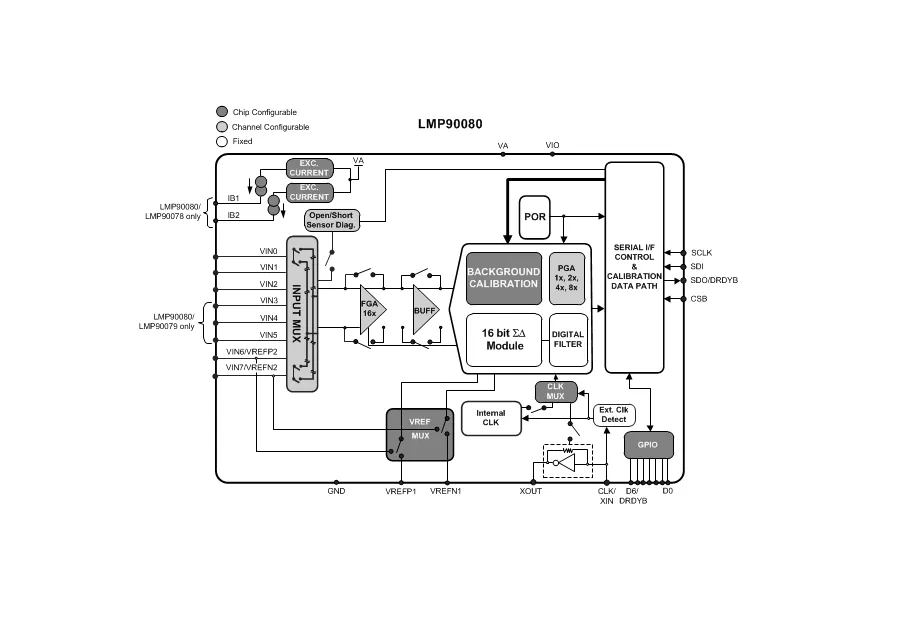
LMP90080-Q1 is a highly integrated multi-channel 16-bit sensor AFE with continuous background calibration, programmable gain, and flexible input configurations. It integrates excitation current sources and sensor diagnostics and is designed for industrial temperature and pressure transmitters, strain gauge interfaces, and other high-precision low-power applications.
Core Parameters and Performance
- Resolution and sampling: 16-bit Sigma-Delta ADC with effective number of bits (ENOB) up to 16; supports 8 ODRs from 1.6775 SPS to 214.65 SPS. When ODR <= 13.42 SPS, 50 Hz/60 Hz line interference is suppressed.
- Gain and noise: Programmable gain 1x–128x (includes fixed 16x amplifier plus programmable 1x/2x/4x/8x stages); total noise < 10 μV-rms; typical offset 8.4 nV; typical gain error 7 ppm.
- Inputs and excitation: Supports 4 differential / 7 single-ended inputs; input impedance 15.4 MΩ; two matched excitation current sources (100 μA–1000 μA, step 100 μA) for RTDs and bridge sensors.
- Power and operating conditions: VA 4.75 V–5.5 V; VIO 2.7 V–5.5 V; typical operating current 464 μA (13.42 SPS); power-down current as low as 4.6 μA; operating temperature -40°C to +150°C.
Package and Pins
- 28-pin HTSSOP (PWP) package with exposed thermal pad. Connect the exposed pad to the PCB ground plane to optimize thermal dissipation.
- Key pins include analog inputs (VIN0–VIN7), reference inputs (VREFP1/VREFN1, VREFP2/VREFN2), excitation outputs (IB1/IB2), SPI interface (SCLK/SDI/SDO/CSB), GPIO pins (D0–D6), and data-ready pin (DRDYB).
Core Functions and Features
- Background and system calibration: Continuous background calibration at all gains to automatically compensate offset and gain drift due to temperature and aging. Built-in system calibration supports in-situ calibration using expected-value programming, with separate offset and gain coefficient configuration.
- Sensor diagnostics: Continuous background detection for open-circuit, short-circuit, and overrange conditions. Built-in 10 μA burn current source. Fault status is reported via flags such as SHORT_THLD_FLAG and RAILS_FLAG.
- Flexible inputs and channel configuration: Input multiplexer supports arbitrary pin combinations as differential or single-ended inputs. Channels can be configured independently for gain and ODR. Supports four channel scan modes (single-channel continuous, multi-channel single/continuous scan, and multi-channel continuous scan with burn current).
- Communication and validation: SPI 3/4-wire interface with CRC data link error detection; maximum SCLK 10 MHz. DRDYB indicates data-ready and can be used as GPIO or as a dedicated output.
Typical Applications
- Temperature and pressure transmitters, RTD interfaces, thermocouple cold-junction compensation (CJC), strain gauge signal acquisition, industrial process control, and PLC analog input modules.
Design Considerations
- Power and decoupling: VA and VIO should be powered independently. Place 0.1 μF ceramic decoupling capacitors close to the device plus a 1 μF tantalum capacitor. Reference voltage pins should have an additional 10 μF tantalum capacitor to reduce supply noise coupling.
- Input and excitation routing: Keep analog input traces short and away from digital circuits. At high gain (>=16x), observe input voltage range (GND + 0.4 V to VA - 1.5 V). When using excitation current sources with external sensors, match lead resistance to maintain accuracy.
- Layout guidelines: Partition PCB into analog and digital areas. Connect analog and digital grounds at a single point. Provide sufficient copper on the thermal pad and stitch to ground with vias. Keep SPI lines isolated from analog input routing.
- Calibration and configuration: Default background calibration mode is BgcalMode2, balancing accuracy and response time. For multi-channel scanning, ScanMode2 or ScanMode3 is recommended to avoid conflicts between calibration and sampling. Configure input pin combinations with CHx_INPUTCN registers and channel gain and ODR with CHx_CONFIG registers.
Part Numbers and Availability
- Available packaging includes tubes (48 parts/tube: LMP90080QMH/NOPB), small reels (250 parts/reel: LMP90080QMHE/NOPB), and large reels (2500 parts/reel: LMP90080QMHX/NOPB). All parts are RoHS compliant. MSL rating 3 (260°C reflow, 168-hour moisture sensitivity).