ALLPCB


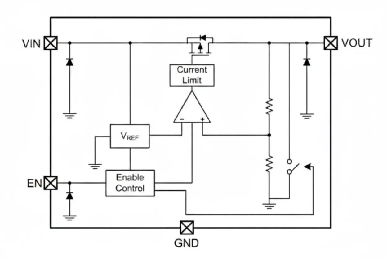
LDO (Low Dropout Regulator) is widely used in embedded systems and is a basic analog power component. Because of its low output noise and simple circuit, it is common in many applications. Several key parameters strongly affect circuit performance; PSRR is one of them.
Key LDO parameters
- PSRR: power supply ripple rejection ratio, i.e., the degree to which ripple at the Vin input is attenuated. A higher value means greater attenuation and better rejection.
- Quiescent current: the current consumed by the regulator itself.
- Output noise: the noise voltage superimposed on the output voltage; lower is better.
- Transient response: the speed of response to changes in load current; faster is better.
- Dropout voltage: the minimum voltage difference (Vin - Vout) required to maintain regulation at the required output current, i.e., the MOSFET voltage drop.
Note: audio systems require low-noise LDOs. Camera sensors typically require LDOs with low noise, high PSRR, and fast transient response.
Design considerations for LDOs
- Place the capacitors for the Vin and Vout pins as close as possible to their respective pins.
- The BP pin may be connected to a capacitor to ground or left unconnected. Connecting a capacitor to ground on BP can improve PSRR by about 2–3 dB.
- For large voltage drops, ensure adequate thermal management, for example by increasing the copper area of the ground plane.
LDO temperature rise calculation
Power dissipation = heating power = (Vin - Vout) * load current.
Temperature rise = power dissipation * thermal resistance.
Temperature rise is the increase in chip temperature caused by heating and does not include ambient temperature. The actual chip temperature = ambient temperature + temperature rise. Therefore, the actual chip temperature depends on PCB thermal design, ambient temperature, and the temperature rise.
The sum of ambient temperature and temperature rise must not exceed the chip junction protection temperature; otherwise the output may shut down.
Thermal resistance depends on the package type. The package defines the thermal resistance and the maximum allowable power for that package.
LDO efficiency
- Exact efficiency for a linear regulator: η = (Vout * Iout) / (Vin * Iin)
- Where Iin = Iout + quiescent current. Because quiescent current is very small (a few microamps to tens of microamps), it can typically be neglected.
- Approximate calculation: η = Vout / Vin