ALLPCB


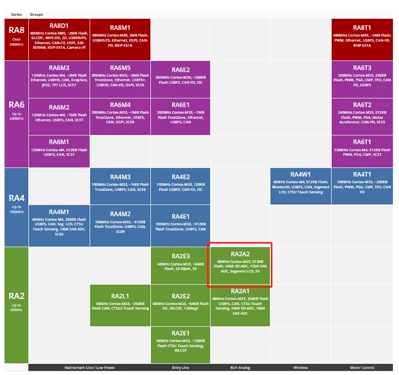
Renesas has added the RA2A2 MCU product group to its RA family. The RA2A2 series is a low-power microcontroller that combines a 48 MHz Arm Cortex-M23 core with a rich set of peripheral functions. This low-power device offers a 24-bit Sigma-Delta analog-to-digital converter (SD-ADC) and an innovative dual-bank code flash with a bank swap function, enabling easy over-the-air (OTA) firmware updates.
The RA2A2 provides multiple power structures and voltage detection hardware to achieve high-efficiency, ultra-low-power operation (as low as 100 μA/MHz in normal mode and 0.40 μA in software standby mode). An independently powered real-time clock (RTC) extends battery life, making it suitable for applications requiring long-term management under extreme conditions. The MCU also provides AES hardware acceleration, a high-precision (±1.0%) high-speed on-chip oscillator, a temperature sensor, and a wide operating voltage range of 1.6V to 5.5V.
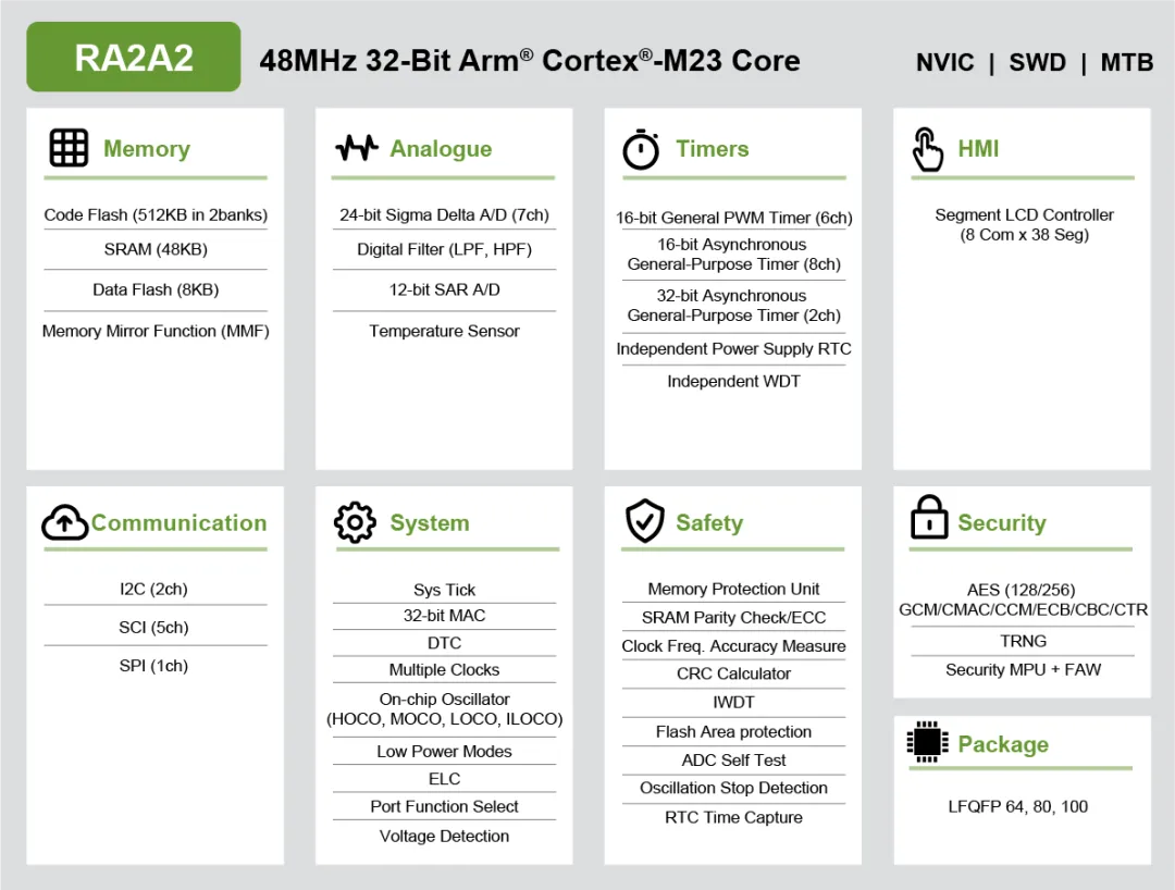
RA2A2 Features
- 48 MHz Arm Cortex-M23 core
- 512KB dual-bank flash memory and 48KB SRAM
- 8KB data flash (100,000 program/erase cycles)
- 64-pin, 80-pin, and 100-pin LFQFP package options
- 24-bit Sigma-Delta A/D converter, 12-bit A/D converter, and temperature sensor
- 16-bit general-purpose timers, 32-bit and 16-bit low-power AGT timers, and an independently powered RTC
- SCI (UART, simple SPI, simple I2C), SPI, and I2C buses
- Segment LCD controller (8com x 38seg)
- Security features, including AES, secure MPU, Flash Access Window, and TRNG
This article focuses on the following three features:
- 24-bit Sigma-Delta A/D converter
- Segment LCD controller (8com x 38seg)
- Dual-bank flash memory
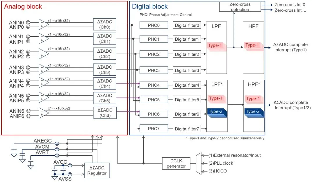
24-Bit Sigma-Delta A/D Converter
The 24-bit SD-ADC achieves low-power and high-precision A/D conversion, suitable for power-sensitive measurement applications.
- Synchronous sampling architecture with up to 7 channels
- Built-in digital filter (LPF+HPF)
Segment LCD Controller (8com x 38seg)
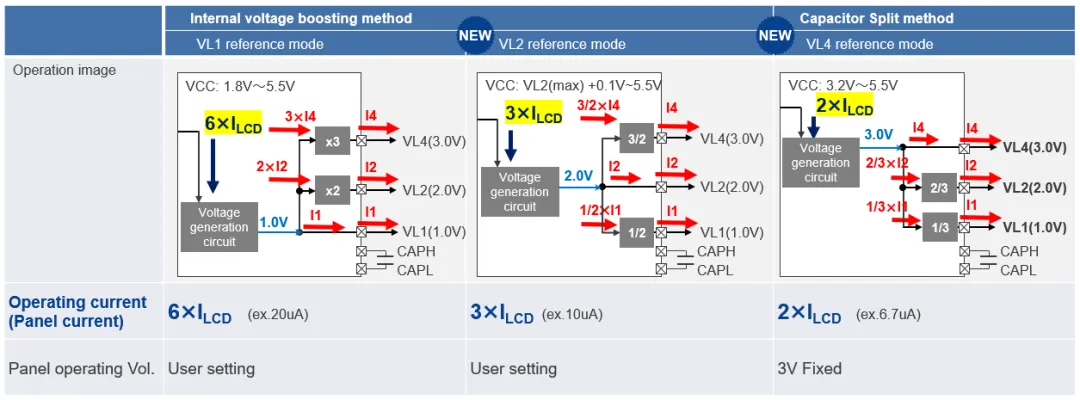
As shown in the figure above, the RA2A2 implements new modes to support system-level low-power operation.
One is the VL2 reference mode, which uses an internal boost method, and the other is the VL4 reference mode, which uses a capacitor-divider method.
Compared to the existing VL1 reference mode, the VL2 reference mode improves the boost efficiency for driving the LCD panel.
In VL1 reference mode, the MCU VCC must first be stepped down to 1.0V and then boosted to 3.0V.
However, the VL2 reference mode saves MCU current because it generates 2.0V as the reference voltage. By increasing the reference voltage from 1.0V to 2.0V, the panel operating current can be halved compared to the VL1 mode, contributing to lower system-level power consumption.
The VL4 reference mode generates 3V in the internal voltage generation circuit, which is then stepped down to produce VL2 and VL1. This allows the VL4 mode to reduce the MCU current used for the LCD panel driver. The panel operating current can be reduced to one-third of that in VL1 mode.
Since the panel drive current significantly impacts the battery life of portable LCD applications, the VL2 and VL4 modes help extend battery life.
Dual-Bank Flash Memory
The RA2A2's flexible dual-bank flash memory facilitates firmware updates via the bank swap function.
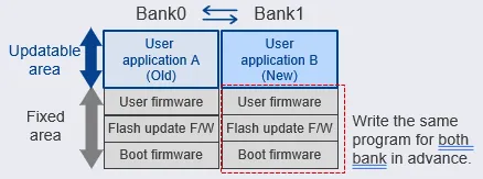
- Both single-bank and dual-bank modes are available (switched via register settings).
- Dual-bank mode simplifies the implementation of firmware updates.
The concept illustrated in the figure is that users can update firmware without interrupting operation.
In summary, the RA2A2 is suitable for smart energy management, building automation, medical equipment, consumer electronics, and other IoT applications that can benefit from firmware updates.