ALLPCB


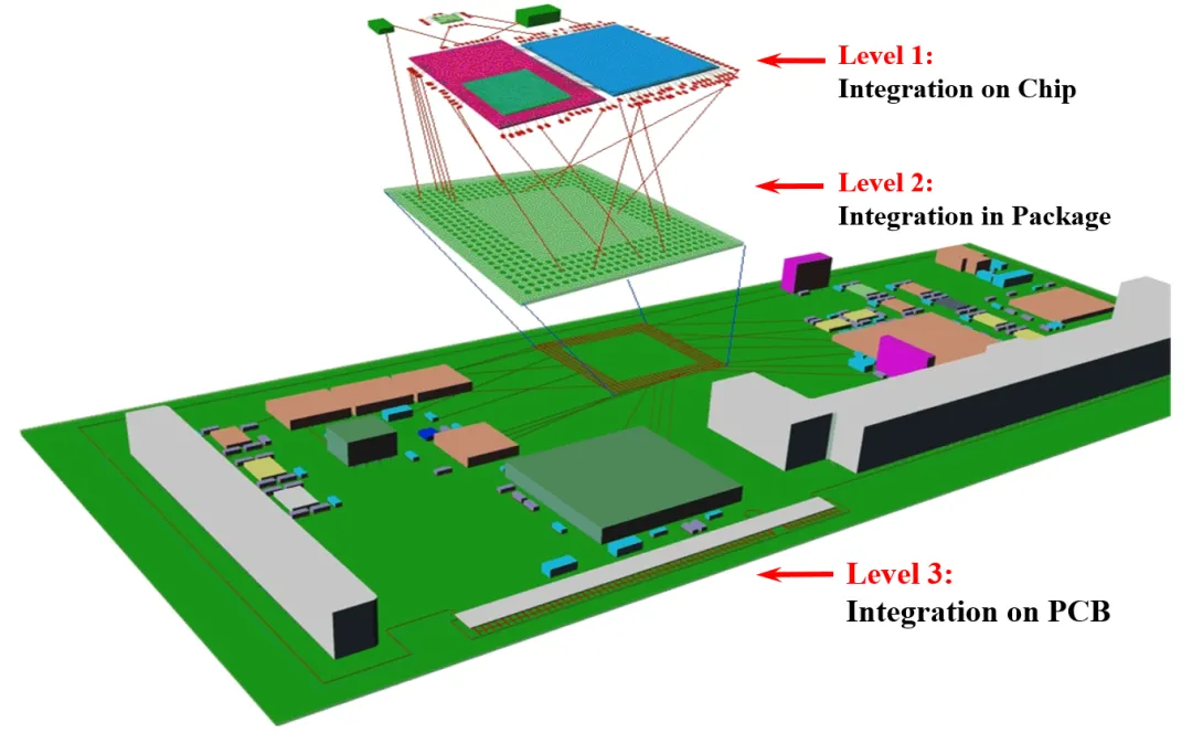
Integration levels
Electronic system integration can be divided into three levels: on-chip integration, in-package integration, and PCB-level integration, as shown below:
The basic units for in-package integration are the bare die or small chiplets produced in the previous step. These functional units are integrated inside the package to form SiP.
On-chip integration
From a simplified perspective, three classes of materials and three types of processes must be understood. Although many materials are used on a chip and modern ICs use elements across the periodic table, they can be categorized into three broad types: conductors, semiconductors, and insulators. Conductors transmit electrons, insulators isolate them, and the semiconductor is the most crucial because it is controllable: it can behave as a conductor (on) or an insulator (off) depending on applied voltages or currents and specific device structures.
Processing, subtractive processes, and pattern transfer
Processing refers to adding material to the substrate. Examples include ion implantation, sputtering, chemical vapor deposition (CVD), and physical vapor deposition (PVD).
Subtractive processes refer to removing material, such as etching, chemical mechanical polishing (CMP), and wafer planarization.
Pattern transfer is the most numerous and challenging category because most add/remove process steps require pattern definition. Pattern transfer means transferring the designed pattern onto the wafer and involves masks, lithography, and photoresist.
The product after these steps is the wafer; once the wafer is diced it yields chips or chiplets ready for the next level of integration.
In-package integration
In-package integration does not rely on semiconductor device action, so materials are mainly conductors and insulators. The goal is to integrate chips or chiplets produced at the previous level and provide electrical interconnection, forming micro-systems represented by SiP and advanced packages.
PCB-level integration
Today PCBs typically use double-sided component mounting and can reach dozens of layers. High-density interconnect (HDI) boards, rigid-flex boards, and microwave circuit boards are widely used. Like in-package integration, PCB integration primarily uses conductors and insulators because semiconductor device behavior is not involved.

Integration stages
Stages of on-chip integration
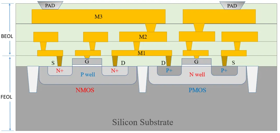
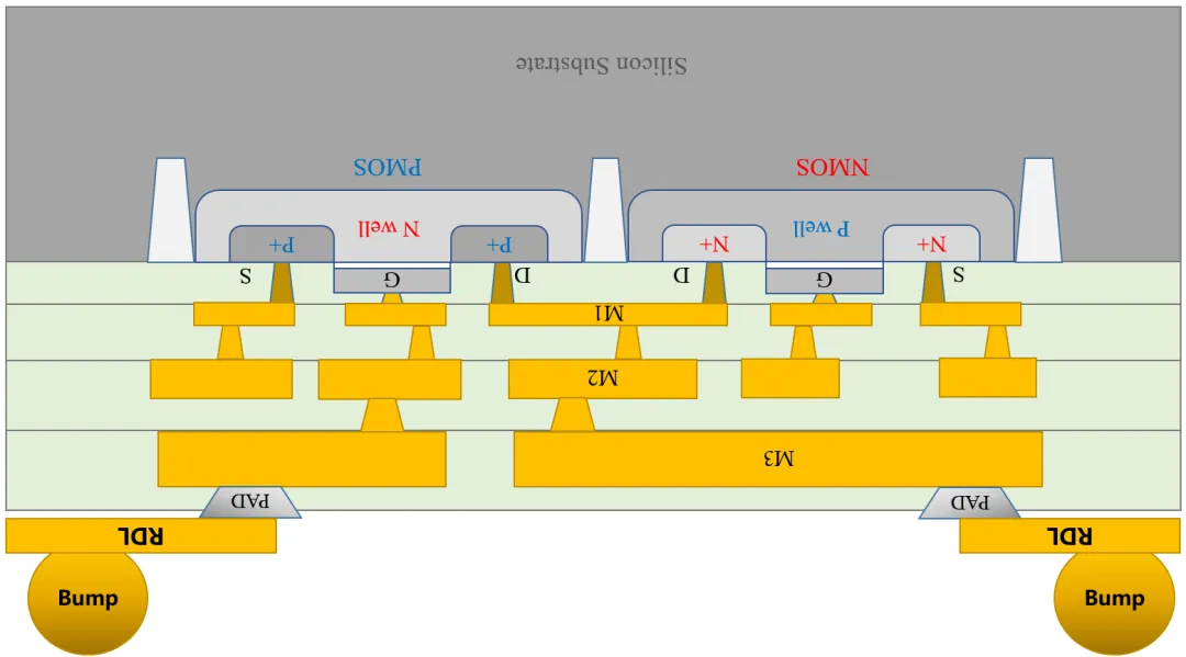
On-chip integration mainly consists of two stages: device fabrication and metal interconnect, commonly referred to as front-end-of-line (FEOL) and back-end-of-line (BEOL).
Device fabrication (FEOL)
Device fabrication forms transistors, resistors, capacitors, diodes, and other functional cells on single-crystal silicon using lithography, etching, ion implantation, sputtering, CVD, PVD, CMP, wafer planarization, and similar steps. Modern 5 nm processes can produce over 100 million transistors per square millimeter.
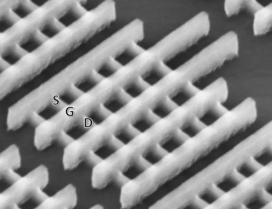
Metal interconnect (BEOL)
After transistor layers are formed, contact holes are made and filled with metals such as tungsten to connect transistors to the first metal layer. Multiple metal routing layers and vias then provide electrical interconnection. Earlier chips used aluminum routing; modern chips predominantly use copper.
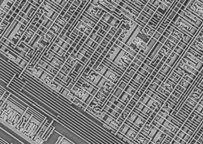
The diagram below shows FEOL and BEOL: transistors are fabricated on the silicon substrate, then connected via metal interconnect and routed out to the chip pads.
Stages of in-package integration
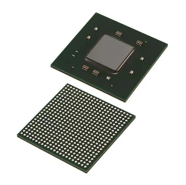
Wire bonding connects chip pads to the package substrate or lead frame, which then connects to external pins. Package types vary by pin arrangement, including BGA, CGA, QFP, LCC, SOP, DIP, and others.
To increase functional density inside the package, more functional units must be integrated. Traditional wire bonding is insufficient for higher densities, which led to the development of advanced packaging techniques. The following sections describe typical methods.
On-chip RDL and TSV fabrication
Redistribution layers (RDL) on the chip surface reroute pads to more convenient locations and form bumps for solder. This extends routing in the XY plane. With bumps, the chip can be mounted directly on a substrate in a flip-chip process.
Since flip-chip parts cannot be stacked vertically, through-silicon via (TSV) technology was developed to create vertical interconnects through the silicon die. TSV presents many processing challenges; two key issues are via placement and reducing via diameter.
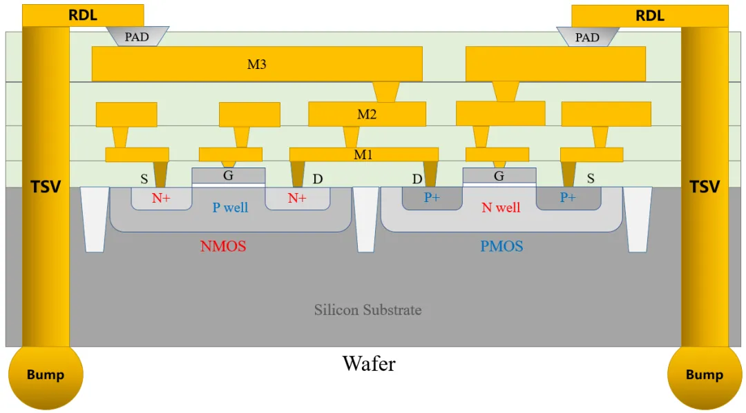
Interposer RDL and TSV fabrication
Package substrates commonly mount components on the top and connect to the board below via BGA.
Component assembly and packaging
Stages of PCB-level integration
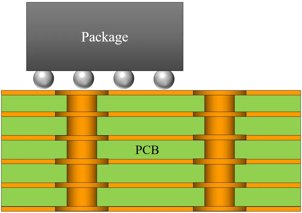
After in-package integration, the assembly footprint is still limited and some discrete components, such as large capacitors and transformers, cannot be included inside the package. Therefore, PCBs remain essential for electronic products.
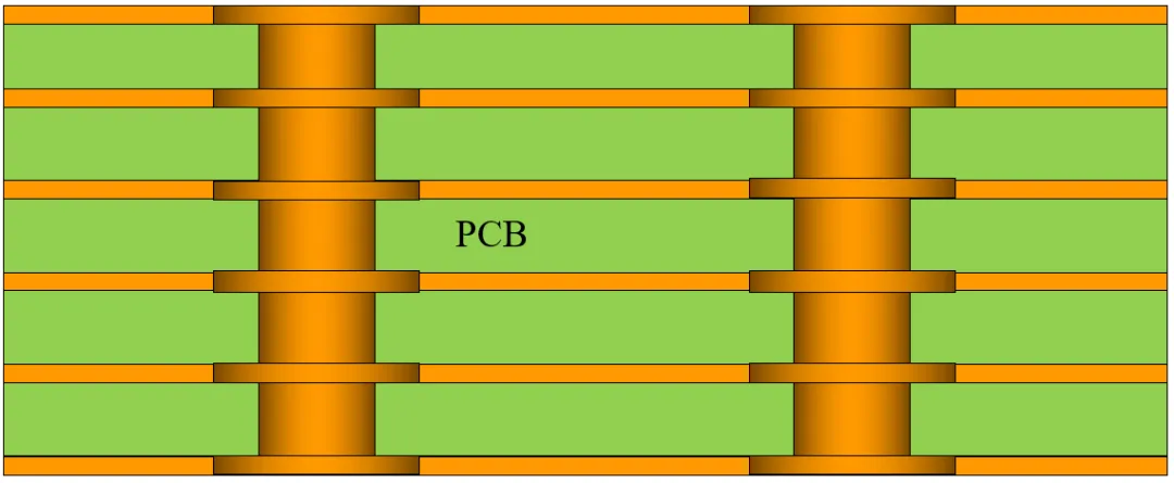
PCB interconnect routing
PCB manufacturing is similar to organic substrates but typically has lower routing density and simpler structures. Many PCBs use through-hole vias; while HDI boards use blind and buried vias, through vias remain common due to simplicity and lower cost. The illustration below shows a 6-layer through-hole PCB used to mount components and provide electrical interconnection.
PCB component assembly
From transistor to PCB
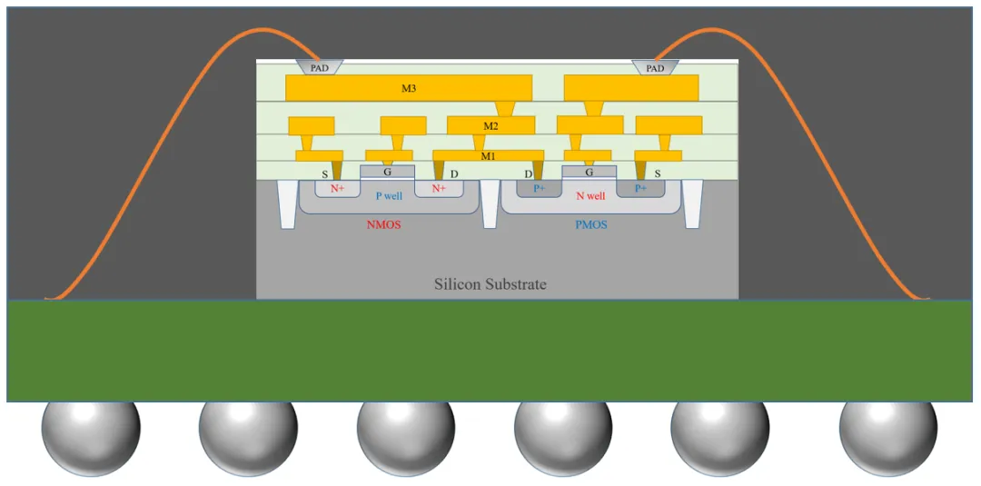
The diagram below summarizes integration from the transistor to the PCB.
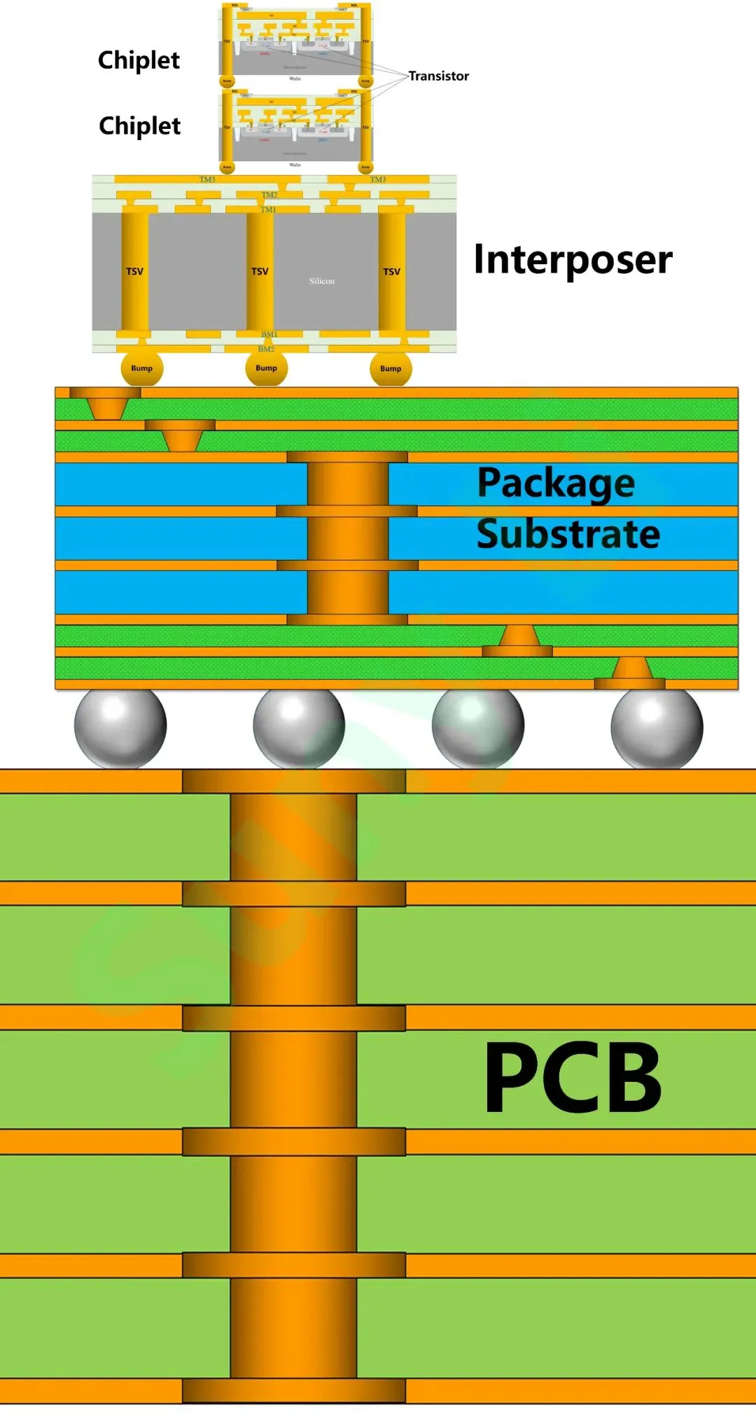
Transistors (NMOS or PMOS) are fabricated on the silicon substrate, connected via contact holes to on-chip metal routing, and routed to chip pads. RDL then connects to 3D TSV and uBumps, which link to silicon interposer RDL and 2.5D TSV. Bumps connect to the package substrate, whose traces and vias lead to a BGA, and finally to PCB routing and vias.