ALLPCB


Circuit and Waveforms
The circuit of an IGBT under a diode-clamped inductive load is shown in Figure 1. This circuit is commonly used to test IGBT switching characteristics and to evaluate turn-on and turn-off behavior. Figure 2 shows the actual IGBT switching waveforms that account for the diode recovery characteristics and stray inductance (Ls); these waveforms can serve as a reference when designing IGBT driver circuits. In the following analysis the IGBT is assumed to operate under steady-state current, with current flowing through an inductive load and then through an ideal freewheeling diode connected in parallel with the load.
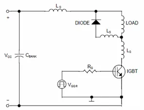
Figure 1. Diode-clamped inductive load
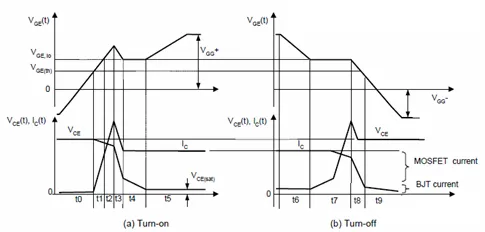
Figure 2. IGBT switching waveforms
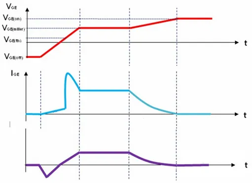
The IGBT turn-on waveform is very similar to that of a MOSFET. The IGBT turn-off characteristics are also similar to a MOSFET except for a tail current. The following sections describe IGBT operation interval by interval.
Turn-on Process
t0 interval
During t0 the gate current iG charges the parasitic capacitances Cge and Cgc, and VGE rises to the threshold VGE(th). VGE can be approximated as rising linearly, but in reality it follows an exponential with time constant RG(Cge + Cgc). During this interval VCE and iC remain essentially constant. Turn-on delay time is defined from when the gate voltage reaches 10% of VGG+ to when the collector current iC reaches 10% of Io. Most of the turn-on delay occurs in t0.
t1 interval
When VGE exceeds VGE(th), a channel forms under the gate oxide and current begins to conduct. In this interval the IGBT operates in the linear region and iC increases with VGE until it reaches the load current Io. VCE decreases slightly relative to Vd due to the stray inductance-induced voltage VLS = LS × diC/dt, which appears across LS opposing Vd. The magnitude of the VCE drop depends on diC/dt and LS, and the waveform shape follows the form of iC.
t2 and t3 intervals
The diode current iD begins to fall during t1 but cannot immediately drop to 0 because of reverse recovery; reverse current flows. The diode reverse recovery current adds to iC, producing similar iC waveforms in t2 and t3. At this time the reverse voltage across the diode increases and VCE falls because Cge has a smaller value at higher VCE, causing a rapid drop in VCE and thus a large dVCE/dt. During t3, Cgc absorbs and emits gate drive current while Cge discharges. At the end of t3 the diode reverse recovery process is complete.
t4 interval
During t4 iG charges Cgc, VGE is held around VGE,Io, and iC remains at the load current Io. VCE falls at a rate approximately equal to (VGG ? VGE,Io)/(RG Cgc). VCE drops significantly and presents a trailing voltage because Cgc is larger at low VCE.
t5 interval
In t5 VGE rises again with time constant RG(Cge + Cgc,miller) until VGG+, where Cgc,miller denotes the Miller capacitance, which increases as VCE decreases. During t5 VCE slowly falls to the collector-emitter saturation voltage as the device fully enters saturation. This behavior arises because the IGBT transistor traverses the linear region more slowly than a MOSFET and because of the Miller capacitance effect.
Turn-off Process
t6 interval
This interval is the turn-off delay. VGE falls from VGG+ to VGE,Io with time constant RG(Cge + Cgc,miller), while VCE and iC remain unchanged.
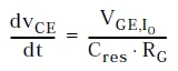
t7 interval
VCE begins to rise in t7; the rise rate can be controlled by RG as given by the relevant expression.
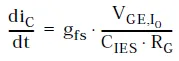
t8 interval
In t8 VCE reaches Vd and iC begins to fall; the fall rate can be controlled by RG as given by the corresponding expression.
As during turn-on, t7 and t8 produce a spike voltage VLS = LS × diC/dt that is superimposed across the collector-emitter terminals of the IGBT. This corresponds to the first of two current-fall stages where the MOSFET-like current component partially disappears. The t9 interval corresponds to the disappearance of the BJT component of iC, commonly called the tail current, which is formed by recombination of injected minority carriers (holes) in the N-drift region. Because of this tail behavior, IGBT switching performance is inferior to that of power MOSFETs.
IGBT Driver Requirements
Key driver requirements include:
- The driver supply energy must at least cover the IGBT drive losses.
- The driver must be capable of supplying the pronounced current spike that occurs at startup.
Common protection functions found in mainstream IGBT drivers are:
- Undervoltage protection, including primary-side input undervoltage and secondary-side (IGBT terminal) undervoltage.
- Short-circuit protection, often implemented as desaturation detection and protection.
- Active clamp and Miller clamp protection.
These protection features are required because of intrinsic IGBT characteristics. An IGBT can be viewed as a MOSFET-based structure combined with a thyristor. The goal is to use the MOSFET-like ease of driving and turn-off together with the ruggedness of a thyristor. However, the IGBT chip is more complex than a MOSFET and therefore exhibits larger parasitic parameters. Since IGBTs are used in high-voltage, high-current applications, high di/dt or dv/dt combined with large parasitics can lead to problems. Consequently, careful work is required on the driver design. The driver itself is a circuit that introduces interference and parasitic elements; under high-frequency common-mode interference these effects can cause IGBT failures. The challenge in IGBT driver design is not the basic principle but in minimizing parasitic parameters and reducing the impact of common-mode interference.