 ALLPCB


When it comes to the manufacturing of printed circuit boards (PCBs), hole size tolerances play a critical role in ensuring the functionality and reliability of the final product. Whether you're designing a simple circuit or a complex multilayer board, understanding hole size tolerances is essential for seamless assembly and performance. In this comprehensive guide, we'll explore what hole size tolerances are, why they matter in PCB manufacturing, and how to specify them correctly for your projects targeting "Hole Size" and "Manufacturing" concerns.
What Are Hole Size Tolerances in PCB Manufacturing?
Hole size tolerances refer to the acceptable range of variation in the diameter of holes drilled into a PCB. These holes serve various purposes, such as mounting components, creating vias for electrical connections between layers, or providing mechanical support. During manufacturing, it’s nearly impossible to drill holes with exact precision every time due to factors like drill bit wear, material properties, and machine limitations. Tolerances define the allowable deviation from the specified hole size to ensure the PCB still functions as intended.
For instance, if a design calls for a hole with a diameter of 0.5 mm, the tolerance might be specified as ±0.05 mm. This means the actual hole size can range from 0.45 mm to 0.55 mm and still be acceptable. Understanding and specifying these tolerances correctly is vital for engineers and designers to avoid issues like poor component fit or electrical failures.
Why Hole Size Tolerances Matter in PCB Manufacturing
Hole size tolerances directly impact the quality and functionality of a PCB. Here are some key reasons why they are crucial:
- Component Fitment: Many components, such as through-hole resistors or connectors, have leads or pins that must fit into the drilled holes. If the hole is too small, the component won’t fit; if it’s too large, the connection may be loose, leading to unreliable soldering or mechanical instability.
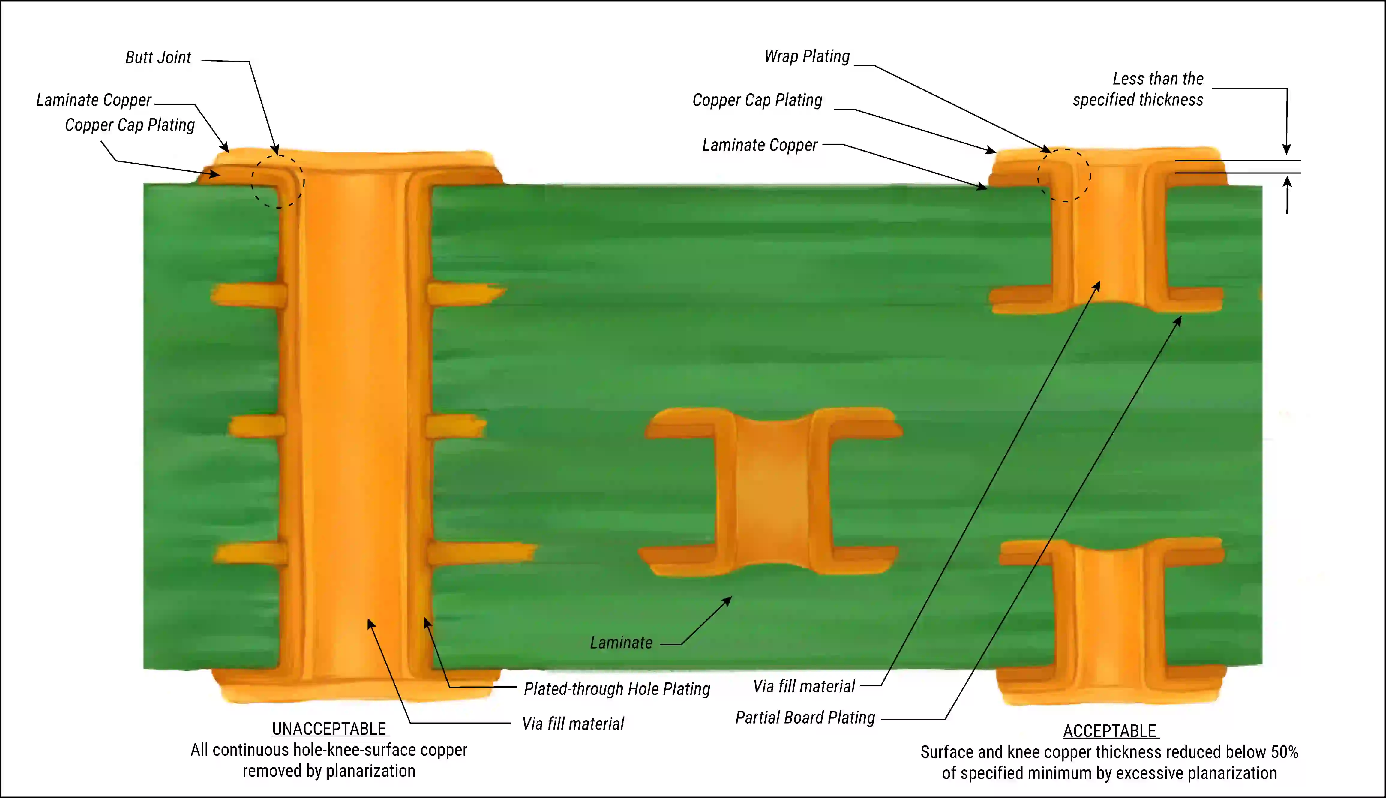
- Electrical Performance: Vias, which are small holes used to connect different layers of a PCB, rely on precise sizing for proper plating and conductivity. Incorrect hole sizes can lead to weak connections or signal integrity issues.
- Manufacturing Efficiency: Specifying realistic tolerances helps manufacturers produce boards without excessive rework or scrap, saving time and cost.
- Mechanical Stability: Holes used for mounting or alignment (often called tooling holes) need accurate sizing to ensure the PCB fits correctly in enclosures or during assembly processes.

Factors Affecting Hole Size Tolerances in PCB Manufacturing
Several factors influence the achievable hole size tolerances during PCB production. Being aware of these can help designers set realistic expectations and specifications.
1. Material Properties
The type of substrate material used in a PCB affects how precisely holes can be drilled. For example, standard FR-4 material, a common choice for many boards, has good dimensional stability and allows for tighter tolerances. On the other hand, high-frequency or specialty materials may have different drilling characteristics, requiring adjusted tolerances or specialized drilling techniques.
2. Board Thickness
Thicker PCBs can pose challenges during drilling due to potential drill bit wander or breakout at the exit point, leading to larger variations in hole size. Conversely, thinner boards might experience stress or deformation during drilling, also affecting precision. For instance, a 1.6 mm thick board might achieve a tolerance of ±0.05 mm, while a 3.2 mm thick board might require ±0.1 mm due to increased drilling challenges.
3. Hole Diameter
Smaller holes are generally harder to drill with tight tolerances. A hole with a diameter of 0.2 mm might have a tolerance of ±0.03 mm, while a larger 2.0 mm hole could achieve ±0.05 mm more consistently. This is because smaller drill bits are more prone to wear and breakage, impacting accuracy.
4. Drilling Equipment and Techniques
The quality of the drilling equipment and the techniques used also play a role. Advanced CNC drilling machines can achieve tighter tolerances compared to older equipment. Additionally, factors like drill bit sharpness, speed, and feed rate can influence the final hole size.
5. Plating and Finishing Processes
After drilling, holes often undergo plating to create conductive paths, especially for vias. The plating process can slightly reduce the hole diameter, typically by 0.025 mm to 0.05 mm, depending on the thickness of the plating. Designers must account for this when specifying tolerances to ensure the finished hole size meets requirements.
Standard Hole Size Tolerances in PCB Manufacturing
While tolerances can vary depending on the manufacturer and project requirements, there are industry-standard ranges that most fabricators adhere to. These standards provide a baseline for designers to work from when specifying hole sizes.
- Non-Plated Through Holes (NPTH): These are holes that do not require plating and are often used for mounting or alignment. Typical tolerances for NPTH are ±0.05 mm to ±0.1 mm, depending on the hole size and board thickness.
- Plated Through Holes (PTH): Used for component leads or vias, PTH tolerances are often tighter due to the need for precise electrical connections. Common tolerances range from ±0.075 mm to ±0.1 mm after plating.
- Vias: Vias are small holes connecting different layers of a PCB. Due to their size (often 0.2 mm to 0.5 mm), tolerances are typically ±0.05 mm to ensure proper plating and conductivity.
These values are general guidelines and may vary based on the capabilities of the manufacturing facility. For critical applications, such as high-speed digital circuits or aerospace components, tighter tolerances (e.g., ±0.025 mm) may be required, often necessitating advanced manufacturing processes and higher costs.
How to Specify Hole Size Tolerances for Your PCB Design
Specifying hole size tolerances correctly in your design files is crucial to avoid miscommunication with the manufacturer. Here are some practical tips to ensure clarity and precision in your specifications:
1. Use Standard Notation
Always specify hole sizes with their nominal diameter and tolerance range. For example, a hole might be noted as 0.8 mm ±0.05 mm. This clearly communicates the acceptable range to the manufacturer.
2. Account for Plating
If the hole will be plated, specify whether the tolerance applies to the drilled size or the finished size after plating. Most manufacturers assume the tolerance is for the finished size unless stated otherwise, so clarify this in your design notes.
3. Reference Component Datasheets
Check the datasheets of components that will be inserted into the holes. These often include recommended hole sizes and tolerances for proper fitment. For example, a resistor lead might have a diameter of 0.6 mm ±0.05 mm, so the hole should be slightly larger, such as 0.7 mm ±0.05 mm, to accommodate it.
4. Communicate with Your Manufacturer
Before finalizing your design, discuss hole size tolerances with your manufacturing partner. They can provide insights into their capabilities and suggest adjustments if your specifications are outside their standard range. This collaboration can prevent delays or quality issues.
5. Include Tolerances in Design Files
Ensure that your PCB design software includes tolerance information in the drill files or fabrication notes. This reduces the risk of misinterpretation during production.
Common Challenges with Hole Size Tolerances and How to Avoid Them
Even with careful planning, issues with hole size tolerances can arise during PCB manufacturing. Here are some common challenges and strategies to mitigate them:
1. Drill Bit Wear
Over time, drill bits wear down, leading to larger holes than intended. To minimize this, manufacturers often use high-quality bits and replace them regularly. As a designer, you can help by specifying slightly looser tolerances for non-critical holes to account for potential wear.
2. Material Deformation
Drilling can cause stress or deformation, especially in thinner boards, resulting in oval or irregular holes. Using appropriate stack-up techniques during drilling and selecting stable materials can reduce this risk.
3. Misalignment
Misalignment of layers or drill positions can lead to holes that don’t match the design. Specifying alignment holes (also called fiducial marks) and ensuring accurate layer registration can help maintain precision.
4. Overly Tight Tolerances
Specifying tolerances that are too tight for standard manufacturing processes can increase costs or lead to rejected boards. Balance the need for precision with practical manufacturing capabilities by consulting with your production team.
Advanced Considerations for Hole Size Tolerances
For high-performance or specialized PCBs, additional considerations may apply when defining hole size tolerances:
- High-Speed Designs: In boards handling high-frequency signals (e.g., above 1 GHz), vias must be precisely sized to minimize signal loss or impedance mismatches. Tolerances as tight as ±0.02 mm may be necessary, often requiring laser drilling instead of mechanical drilling.
- Thermal Management: Holes used for heat dissipation, such as thermal vias under power components, need consistent sizing to ensure effective heat transfer. Variations in hole size can impact thermal performance.
- Microvias: In advanced designs like HDI (High-Density Interconnect) boards, microvias with diameters as small as 0.1 mm are used. These require extremely tight tolerances (e.g., ±0.01 mm) and specialized manufacturing processes.
Conclusion: Mastering Hole Size Tolerances for PCB Success
Hole size tolerances are a fundamental aspect of PCB manufacturing that can make or break the performance of your design. By understanding the factors that influence tolerances, adhering to industry standards, and communicating effectively with your manufacturing partner, you can ensure that your PCBs meet both functional and quality requirements. Whether you're working on a simple prototype or a complex high-speed board, paying attention to "Hole Size" and "Manufacturing" specifications will lead to better outcomes and smoother production processes.
At ALLPCB, we’re committed to helping you achieve precision and reliability in every project. By incorporating these best practices into your designs, you’ll be well-equipped to tackle the challenges of PCB manufacturing with confidence.


