The classification of semiconductor materials into first, second, and third generations does not imply that later generations are inherently superior. In China, the term "third-generation semiconductors" refers to materials driving the third wave of industrial revolutions enabled by large-scale semiconductor applications. Internationally, materials like gallium nitride (GaN) and silicon carbide (SiC) are often categorized as wide-bandgap semiconductors, nitride semiconductors (e.g., GaN, AlN, InN), or III-V semiconductors (e.g., GaN, GaAs, InP). Currently, third-generation semiconductors are rapidly advancing, while first- and second-generation materials continue to play critical, irreplaceable roles in various industries. This article explores the technical distinctions between the three generations, their advancements, and the prominence of GaN and SiC in third-generation applications.
Technical Distinctions Between Semiconductor Generations
1. Materials
First-generation semiconductors, introduced in the 1950s, are represented by silicon (Si) and germanium (Ge). Silicon, in particular, forms the foundation of logic devices, enabling the computational power of CPUs and GPUs. Second-generation semiconductors, developed in the 1980s, consist of compound semiconductors, primarily gallium arsenide (GaAs) and indium phosphide (InP). GaAs is critical for radio frequency (RF) power amplifiers, while InP is widely used in optical communication devices. Third-generation semiconductors, which emerged in the early 2000s century, include silicon carbide (SiC), gallium nitride (GaN), zinc oxide (ZnO), diamond (C), and aluminum nitride (AlN). These materials are characterized by wide bandgaps (Eg > 2.3 eV), earning them the designation as wide-bandgap semiconductors.
2. Bandgap
First-generation semiconductors have indirect, narrow bandgaps. Second-generation materials feature direct, narrow bandgaps. In contrast, third-generation semiconductors possess wide bandgaps with direct bandgap characteristics across all compositions. Compared to traditional semiconductors, wider bandgaps enable operation at higher temperatures, voltages, and switching frequencies.
3. Applications
First-generation semiconductors are primarily used in discrete devices and chip manufacturing. Second-generation materials are employed in high-speed, high-frequency, high-power, and light-emitting devices, making them ideal for high-performance microwave and millimeter-wave components. They are widely applied in microwave communication, optical communication, satellite communication, optoelectronic devices, lasers, and satellite navigation. Third-generation semiconductors are utilized in high-temperature, high-frequency, high-power, and radiation-resistant devices, supporting applications in semiconductor lighting, 5G communication, satellite communication, optical communication, power electronics, and aerospace.
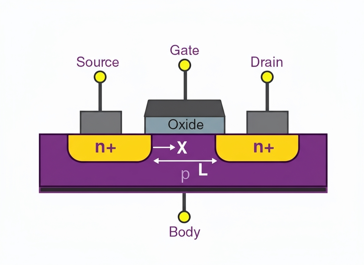
Third-generation semiconductors are recognized as a new driver of the electronics industry. For instance, silicon carbide (SiC) offers high critical electric field strength, high electron saturation velocity, and excellent thermal conductivity, making its devices suitable for high-frequency, high-temperature applications. Compared to silicon devices, SiC components significantly reduce switching losses, enabling high-voltage, high-power devices like MOSFETs, IGBTs, and Schottky barrier diodes (SBDs) for smart grids and electric vehicles. Gallium nitride (GaN), with its high critical electric field, high electron saturation velocity, and exceptional electron mobility, is ideal for ultra-high-frequency devices in 5G communication and microwave RF applications. Third-generation materials can reduce energy losses by over 50% compared to silicon-based semiconductors while decreasing equipment size by more than 75%. These materials align with post-Moore's Law concepts, with lower process and equipment requirements but challenges in material preparation and design optimization.
Current State of Third-Generation Semiconductors
Due to limitations in manufacturing equipment, processes, and costs, third-generation semiconductors have historically been confined to niche applications, unable to challenge silicon's dominance. However, progress has been made in China, where 4-inch SiC substrates are now in mass production, and 6-inch substrate development is complete. For GaN, Chinese companies can produce 2-inch substrates in small batches, have achieved 4-inch substrate production capabilities, and have developed 6-inch prototypes. Advancements in preparation techniques continue to address these challenges.
Opportunities for Third-Generation Semiconductors
Driven by emerging demands in 5G and electric vehicles, third-generation semiconductors are poised for accelerated growth. Silicon-based semiconductors struggle to meet the performance requirements of these applications, amplifying the advantages of SiC and GaN. Additionally, improvements in manufacturing have reduced the costs of SiC and GaN devices, enhancing their cost-effectiveness. The core growth areas for third-generation semiconductors are expected to center on applications where SiC and GaN excel.
Third-Generation Semiconductors: Gallium Nitride (GaN)
GaN devices encompass RF components, power electronics, and optoelectronic devices. Commercial applications began with LED lighting and lasers, leveraging GaN's direct bandgap and spectral properties, with these sectors now highly mature. RF and power devices are the primary areas exploiting GaN's wide-bandgap characteristics. Key advantages include compact size, high-frequency high-power operation, low energy consumption, and fast performance. The 5G communication market is a major growth driver for GaN RF devices, as 5G base stations utilize multiple-input multiple-output (MIMO) antenna arrays, where GaN RF components significantly reduce power consumption and system size. In high-power, high-frequency RF applications, GaN enables higher bandwidth, faster data rates, and lower system power usage. Additionally, GaN RF power transistors can serve as solid-state microwave energy sources, replacing traditional 2.45 GHz magnetrons in applications from microwave ovens to high-power industrial welding.
Third-Generation Semiconductors: Silicon Carbide (SiC)
SiC development began in the 1970s, with commercial SiC Schottky barrier diodes (SBDs) introduced in 2001 and SiC MOSFETs in 2010. SiC IGBTs remain in development. SiC devices offer lower switching losses in power conversion, improving energy efficiency, enabling module miniaturization, and supporting high-temperature operation. Primary applications include smart grids, transportation, electric vehicles, photovoltaics, and wind power, with electric vehicles being the main growth driver. SiC devices are used in power control units (PCUs), inverters, DC-DC converters, and onboard chargers in electric vehicles, enhancing performance and efficiency.
 ALLPCB


