In the world of PCB manufacturing, two concepts stand out as critical to success: Design for Testability (DFT) and Design for Manufacturability (DFM). But what exactly are DFT and DFM, and how do they work together to streamline the PCB manufacturing process? Simply put, DFT focuses on making a printed circuit board (PCB) easy to test for faults, while DFM ensures the design is optimized for efficient production and assembly. Together, they form a powerful approach to reduce costs, improve quality, and speed up time-to-market. In this blog, we’ll explore how these methodologies synergize, dive into practical DFM guidelines, and highlight their impact on design for assembly and the overall PCB manufacturing process.
What Are DFT and DFM in PCB Manufacturing?
Before we dive deeper, let’s break down these two essential concepts. DFT, or Design for Testability, refers to designing a PCB in a way that makes it easier to test for defects during and after production. This could mean adding test points to check signal integrity or ensuring key components are accessible for probing. On the other hand, DFM, or Design for Manufacturability, involves creating a PCB layout that simplifies the manufacturing and assembly process. This includes considerations like component spacing, trace widths, and material choices to avoid production issues.
When combined, DFT and DFM create a holistic approach to PCB design. They ensure that a board isn’t just easy to build but also reliable and testable, saving time and money in the long run. Let’s explore how these principles work together and why they matter for anyone involved in PCB development.
Why DFT and DFM Matter in PCB Manufacturing
The PCB manufacturing process is complex, involving multiple stages like design, fabrication, assembly, and testing. Errors or inefficiencies at any stage can lead to costly rework, delays, or product failures. Studies suggest that testing alone can account for 25-30% of the total cost of producing a PCB. Meanwhile, poor design choices can increase manufacturing scrap rates by up to 10%. This is where DFT and DFM come in—they address these pain points by optimizing the design for both production and quality assurance.
For instance, a PCB designed with DFT in mind might include dedicated test pads for checking a critical signal path with a 50-ohm impedance. This small addition can make it easier to detect issues like signal degradation during testing. Similarly, a DFM-focused design might use a minimum trace width of 6 mils to ensure the board can be fabricated without risking shorts or breaks during etching. By integrating these practices early in the design phase, manufacturers can avoid expensive mistakes and ensure a smoother production cycle.
The Synergy Between DFT and DFM
While DFT and DFM have distinct goals, they often overlap in their implementation. A design choice that benefits manufacturability can also improve testability, and vice versa. Let’s look at a few ways these two approaches complement each other:
- Component Placement: Placing components with enough spacing (e.g., at least 0.5 mm apart) not only makes assembly easier (a DFM principle) but also ensures test probes can access key areas without interference (a DFT benefit).
- Test Points: Adding test points for critical nets, such as a high-speed signal running at 2.5 GHz, helps in fault detection (DFT) and can also guide manufacturers in aligning assembly processes (DFM).
- Standardized Materials: Using widely available materials like FR-4 with a dielectric constant of 4.5 supports cost-effective production (DFM) and ensures consistent test results (DFT).
By considering both DFT and DFM during the design phase, engineers can create PCBs that are not only easier to build and assemble but also more reliable when tested. This synergy reduces the likelihood of design iterations and speeds up the path from prototype to production.
Key DFM Guidelines for PCB Manufacturing
To achieve the benefits of DFM, designers must follow specific guidelines that optimize the PCB for manufacturing and assembly. Below are some practical DFM tips tailored for the PCB manufacturing process:
1. Optimize Trace Widths and Spacing
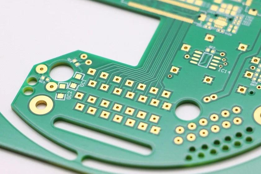
Ensure that trace widths and spacing meet the capabilities of standard fabrication processes. For example, a minimum trace width of 6 mils and spacing of 6 mils is often recommended for most manufacturers to prevent issues like over-etching or short circuits. Narrower traces might be feasible for high-density designs, but they increase production risks and costs.
2. Use Standard Component Sizes
Stick to standard component packages like 0603 or 0805 for resistors and capacitors. Non-standard sizes can complicate assembly and increase the risk of errors during pick-and-place operations. This also aligns with design for assembly principles by ensuring compatibility with automated equipment.
3. Minimize Layer Count
While multi-layer boards are sometimes necessary for complex designs, reducing the number of layers (e.g., from 8 to 6) can lower fabrication costs. Each additional layer adds to the manufacturing time and material expenses, so balance performance needs with cost efficiency.
4. Avoid Tight Tolerances Unless Necessary
Over-specifying tolerances, such as requiring a via diameter of exactly 0.3 mm instead of a more flexible range, can drive up costs. Most standard processes can achieve tolerances of ±10%, so design within these limits unless tighter specs are critical for performance.
5. Provide Clear Silkscreen Markings
Include clear and legible silkscreen labels for components, test points, and polarity markers. This helps during assembly and testing, reducing the chance of errors. Keep text at least 0.8 mm tall to ensure readability after printing.
Following these DFM guidelines not only simplifies the PCB manufacturing process but also sets the stage for effective DFT implementation, as a well-manufactured board is easier to test and debug.
Integrating DFT into Your PCB Design
While DFM focuses on ease of production, DFT ensures that the final product can be thoroughly tested for functionality and reliability. Here are some key strategies to incorporate DFT into your design:
1. Add Accessible Test Points
Include test points for critical signals, such as a clock line operating at 100 MHz, to allow easy probing during testing. Place these points on the top or bottom layer, away from dense component areas, with a minimum pad size of 1 mm for probe contact.
2. Design for Boundary Scan Testing
Incorporate boundary scan architecture (JTAG) for complex designs with multiple ICs. This allows testing of interconnections without physical probing, saving time and reducing the risk of damage during testing.
3. Ensure Power and Ground Access
Provide dedicated test points for power and ground nets to verify voltage levels (e.g., ensuring a 3.3V rail is within ±5% tolerance). This helps identify power-related issues early in the testing phase.
By embedding these DFT practices, you can catch defects like open circuits or incorrect signal levels before the PCB reaches the end user, ensuring higher quality and reliability.
Design for Assembly: Bridging DFM and DFT
Design for Assembly (DFA) is closely tied to DFM and plays a vital role in the PCB manufacturing process. DFA focuses on simplifying the assembly of components onto the PCB, which can indirectly support DFT goals. For example:
- Component Orientation: Align components like diodes or polarized capacitors in the same direction to speed up assembly and reduce errors. This also makes it easier to test for correct placement during quality checks.
- Panelization: Design the PCB to fit into a panel layout with breakaway tabs spaced at least 2.5 mm apart. This aids in efficient assembly and allows for easier testing of multiple boards at once.
- Solder Mask Clearance: Maintain a solder mask clearance of 0.1 mm around pads to prevent solder bridging during assembly. This ensures cleaner joints that are easier to inspect during testing.
By integrating DFA with DFM and DFT, you create a design that’s not only easy to build and test but also quick to assemble, further reducing production time and costs.
Challenges in Balancing DFT and DFM
While DFT and DFM are complementary, balancing the two can sometimes pose challenges. For instance, adding numerous test points for DFT might clutter the board, making it harder to meet DFM spacing requirements. Similarly, minimizing layer count for DFM could limit routing options, complicating DFT strategies like boundary scan implementation.
To overcome these challenges, prioritize critical design needs based on the project’s goals. If reliability is paramount, allocate more space for test points. If cost is the primary concern, focus on simplifying the design for manufacturing. Collaboration between design and manufacturing teams is also key—early feedback can help identify potential conflicts and find solutions before production begins.
Tools and Technologies Supporting DFT and DFM
Modern design software offers powerful features to integrate DFT and DFM into the PCB development process. These tools can run simulations to check for manufacturability issues, such as trace widths below 5 mils, or highlight areas lacking test points for critical nets. They can also generate reports on assembly risks, like components placed too close together (less than 0.3 mm apart), helping designers address issues before fabrication.
Using such tools ensures that both DFT and DFM principles are applied consistently, reducing the likelihood of costly redesigns. They also enable real-time collaboration between engineers and manufacturers, ensuring everyone is aligned on design goals.
Conclusion: Building Better PCBs with DFT and DFM
In the fast-paced world of electronics, delivering high-quality PCBs on time and within budget is more important than ever. By adopting a synergistic approach to DFT and DFM, designers can create boards that are easier to manufacture, assemble, and test. Following DFM guidelines—like optimizing trace spacing and using standard components—ensures a smooth production process, while DFT strategies—such as adding test points and supporting boundary scan—guarantee reliability and performance.
Whether you’re working on a simple single-layer board or a complex multi-layer design, integrating these principles into your workflow can save time, reduce costs, and improve product quality. Start by reviewing your current designs for DFT and DFM opportunities, and leverage modern tools to streamline the process. With this combined approach, you’ll be well-equipped to tackle the challenges of PCB manufacturing and deliver outstanding results.
 ALLPCB


