ALLPCB


In the fast-evolving world of electronics, designing a printed circuit board (PCB) for LCD (Liquid Crystal Display) technology can be a complex puzzle. Whether you're working on consumer gadgets, industrial equipment, or automotive displays, understanding LCD PCB design considerations is crucial for creating reliable and high-performing systems. This blog post will guide you through the essentials of integrating LCD technology into PCB design, covering key topics like LCD impedance matching on PCB, minimizing EMI in LCD circuits, LCD PCB stackup guidelines, and high-speed LCD interface design. Let’s dive into the details to help you master these concepts and optimize your designs for success.
Why LCD Technology Matters in PCB Design
LCDs are everywhere—think smartphones, TVs, medical devices, and even car dashboards. Their ability to display clear, vibrant images with low power consumption makes them a top choice for modern electronics. However, integrating an LCD into a PCB isn’t as simple as connecting a few wires. The design must account for signal integrity, electromagnetic interference (EMI), and high-speed data transfer to ensure the display works flawlessly.
For engineers, the challenge lies in balancing performance with practicality. A poorly designed PCB can lead to flickering displays, distorted images, or even complete system failures. That’s why understanding the nuances of LCD technology and applying the right design principles is so important. Let’s break down the critical aspects of designing a PCB for LCD applications.
Key LCD PCB Design Considerations
When designing a PCB for an LCD, several factors come into play. These considerations ensure that the display operates correctly and integrates seamlessly with the rest of the system. Here are the main points to keep in mind:
- Power Supply Stability: LCDs often require multiple voltage levels for the backlight, driver circuits, and logic. Ensure your PCB design includes stable power rails with proper decoupling capacitors (e.g., 0.1 μF ceramic capacitors near IC pins) to filter out noise.
- Signal Integrity: LCDs rely on precise timing and data signals. Any delay or distortion can cause display issues. Use controlled trace lengths and avoid sharp bends in critical signal paths.
- Connector Compatibility: Choose connectors that match the LCD’s interface (e.g., FPC or pin headers) and ensure they are rated for the required current and voltage.
- Thermal Management: Backlights and driver circuits can generate heat. Design your PCB with adequate copper planes or vias to dissipate heat and prevent overheating.
By addressing these factors early in the design process, you can avoid common pitfalls and create a robust foundation for your LCD integration.
LCD Impedance Matching on PCB: Why It Matters
Impedance matching is a critical concept in PCB design, especially when dealing with high-speed signals often found in LCD interfaces. LCD impedance matching on PCB ensures that the signal energy is transferred efficiently between the driver IC and the display, minimizing reflections and signal loss.
For most LCDs, data and clock signals operate at frequencies ranging from 10 MHz to over 100 MHz, depending on the resolution and refresh rate. At these speeds, mismatched impedance can cause signal reflections, leading to data errors or display glitches. A common target impedance for high-speed digital signals is 50 ohms for single-ended traces and 100 ohms for differential pairs.
To achieve proper impedance matching, follow these steps:
- Calculate Trace Width: Use an impedance calculator based on your PCB material’s dielectric constant (Dk, typically around 4.2 for FR-4) and the desired impedance. For a 50-ohm trace on a standard 1.6 mm FR-4 board, the trace width might be around 0.3 mm.
- Maintain Consistent Spacing: Keep traces at a uniform distance from the reference ground plane to avoid impedance variations.
- Use Termination Resistors: For critical lines, add series or parallel termination resistors (e.g., 33 ohms or 50 ohms) near the receiver to dampen reflections.
By carefully designing your traces for impedance matching, you’ll ensure clean signal transmission and a stable LCD performance.
Minimizing EMI in LCD Circuits: A Must for Reliability
Electromagnetic interference (EMI) can wreak havoc on LCD circuits, causing flickering, noise, or even data corruption. Minimizing EMI in LCD circuits is essential to maintain display quality and ensure compliance with regulatory standards.
EMI often originates from high-speed switching signals, power supply noise, or external sources. Since LCDs use fast data rates and sensitive analog components, they are particularly vulnerable. Here are proven strategies to reduce EMI in your PCB design:
- Ground Plane Design: Use a solid, unbroken ground plane beneath signal layers to provide a low-impedance return path for currents. Avoid splitting the ground plane under high-speed traces.
- Shielding: Place sensitive LCD signal traces between ground planes in a multilayer PCB to shield them from external interference.
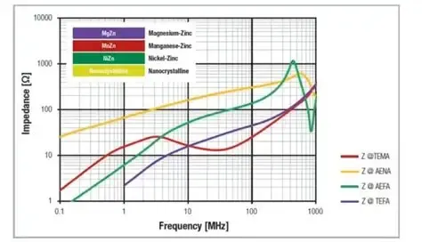
- Filter High-Frequency Noise: Add ferrite beads (e.g., 600 mA, 120 ohms at 100 MHz) and bypass capacitors on power lines near the LCD driver to suppress noise.
- Shorten Trace Lengths: Keep high-speed signal traces as short as possible to reduce the loop area and minimize radiated emissions.
Implementing these techniques will significantly cut down EMI, ensuring your LCD operates smoothly even in noisy environments.
LCD PCB Stackup Guidelines: Building a Strong Foundation
A well-planned PCB stackup is the backbone of any high-performance design, especially for LCD applications. LCD PCB stackup guidelines help ensure signal integrity, power distribution, and EMI control by defining the arrangement of copper and dielectric layers.
For LCD designs, a multilayer PCB (4 or 6 layers) is often recommended to accommodate high-speed signals and provide adequate grounding. Here’s a typical 6-layer stackup for an LCD PCB:
- Layer 1: Top Signal (LCD data and control signals)
- Layer 2: Ground Plane
- Layer 3: Power Plane (for LCD driver and backlight)
- Layer 4: Internal Signal (additional routing if needed)
- Layer 5: Ground Plane
- Layer 6: Bottom Signal (secondary signals or test points)
This stackup provides dedicated ground planes for shielding and separates power and signal layers to reduce crosstalk. Keep the dielectric thickness between layers consistent (e.g., 0.2 mm for high-speed designs) to maintain impedance control. Also, ensure that high-speed LCD signals are routed on layers adjacent to a ground plane for a stable reference.
By following these stackup guidelines, you’ll create a PCB that supports the demands of LCD technology while minimizing potential issues.
High-Speed LCD Interface Design: Meeting Performance Demands
Modern LCDs often use high-speed interfaces like LVDS (Low-Voltage Differential Signaling), MIPI DSI (Display Serial Interface), or RGB parallel interfaces to transmit data at rates exceeding 100 Mbps. High-speed LCD interface design requires careful attention to ensure data integrity and timing accuracy.
Here are the key principles for designing high-speed LCD interfaces on a PCB:
- Differential Pair Routing: For interfaces like LVDS or MIPI, route differential pairs with equal lengths and tight coupling (e.g., 0.1 mm spacing between traces) to maintain signal synchronization. Keep length mismatches under 5 mils (0.127 mm) to avoid skew.
- Clock Signal Protection: Isolate clock signals from other high-speed lines to prevent crosstalk. Surround them with ground vias if possible.
- Timing Constraints: Ensure that data and clock signals meet the LCD’s setup and hold time requirements. For example, a typical MIPI DSI interface might require a setup time of 1 ns at 800 Mbps.
- Via Minimization: Reduce the number of vias on high-speed traces, as they introduce impedance discontinuities. If vias are necessary, use back-drilling to remove unused stubs.
Designing for high-speed interfaces is all about precision. By adhering to these rules, you’ll ensure that your LCD receives clean, accurate data for a flawless display output.
Practical Tips for Successful LCD PCB Design
Beyond the technical details, here are some practical tips to streamline your LCD PCB design process and avoid common mistakes:
- Start with a Schematic: Create a detailed schematic that includes all LCD connections, power requirements, and interface specifications before moving to layout.
- Simulate Signal Integrity: Use simulation tools to analyze signal behavior and impedance before manufacturing. This can save time and costly revisions.
- Test with Prototypes: Build and test a prototype to validate your design under real-world conditions. Check for EMI issues, display artifacts, or thermal problems.
- Follow Manufacturer Guidelines: Always refer to the LCD module’s datasheet for specific design recommendations, such as pin assignments or timing diagrams.
These steps will help you refine your design and achieve a reliable, high-quality result.
Conclusion: Mastering LCD Technology in PCB Design
Designing a PCB for LCD technology is a multifaceted challenge that requires attention to detail and a solid understanding of key principles. By focusing on LCD PCB design considerations, achieving LCD impedance matching on PCB, minimizing EMI in LCD circuits, following LCD PCB stackup guidelines, and optimizing high-speed LCD interface design, you can create a PCB that meets the demands of modern display applications.
At ALLPCB, we’re committed to supporting engineers with the tools and resources needed to bring innovative designs to life. Whether you’re tackling a simple monochrome display or a complex high-resolution panel, applying the strategies outlined in this guide will set you on the path to success. Keep experimenting, refining, and pushing the boundaries of what’s possible with LCD technology in your PCB designs.