In circuit design, different chips operate at varying voltage levels, such as 1.8V, 3.3V, or 5V. To enable communication between devices with different voltage levels, level conversion is necessary to match the signal voltages. This article introduces common level conversion methods used in electronics.
Diode-Based Level Conversion
A typical approach uses a pull-up resistor combined with a diode.
Applicable Scenarios
This method is suitable for circuits where the input signal voltage is higher than the output signal voltage.
Advantages
- Low cost
- Minimal component count
Disadvantages
- Supports only unidirectional signal transmission
- Requires input signal voltage to be higher than output signal voltage
- Diode introduces significant voltage drop
To minimize signal errors due to voltage drop, select a Schottky diode with a low forward voltage drop.
Operational Analysis
When a 3.3V device outputs a high signal, a 5V pull-up resistor raises the input device signal to 5V. When the 3.3V device outputs a low signal, the output signal is pulled low, resulting in a low signal at the input device.
Transistor-Based Level Conversion
This method employs a transistor-based circuit for level conversion.
Applicable Scenarios
Suitable for circuits where the input signal voltage exceeds the output signal voltage.
Advantages
- Low cost
- Minimal component count
- Can be driven with lower input current compared to diode-based circuits, offering an advantage for peripherals with weak drive capabilities
Disadvantages
- Supports only unidirectional signal transmission
- Requires input signal voltage to be higher than output signal voltage
- Transistor PN junction introduces a voltage drop
Select a transistor with a low conduction voltage drop to minimize signal distortion.
Operational Analysis
When a 3.3V device outputs a high signal, a 5V pull-up resistor raises the input device signal to 5V. When the 3.3V device outputs a low signal, the PNP transistor conducts, pulling the input device signal low.
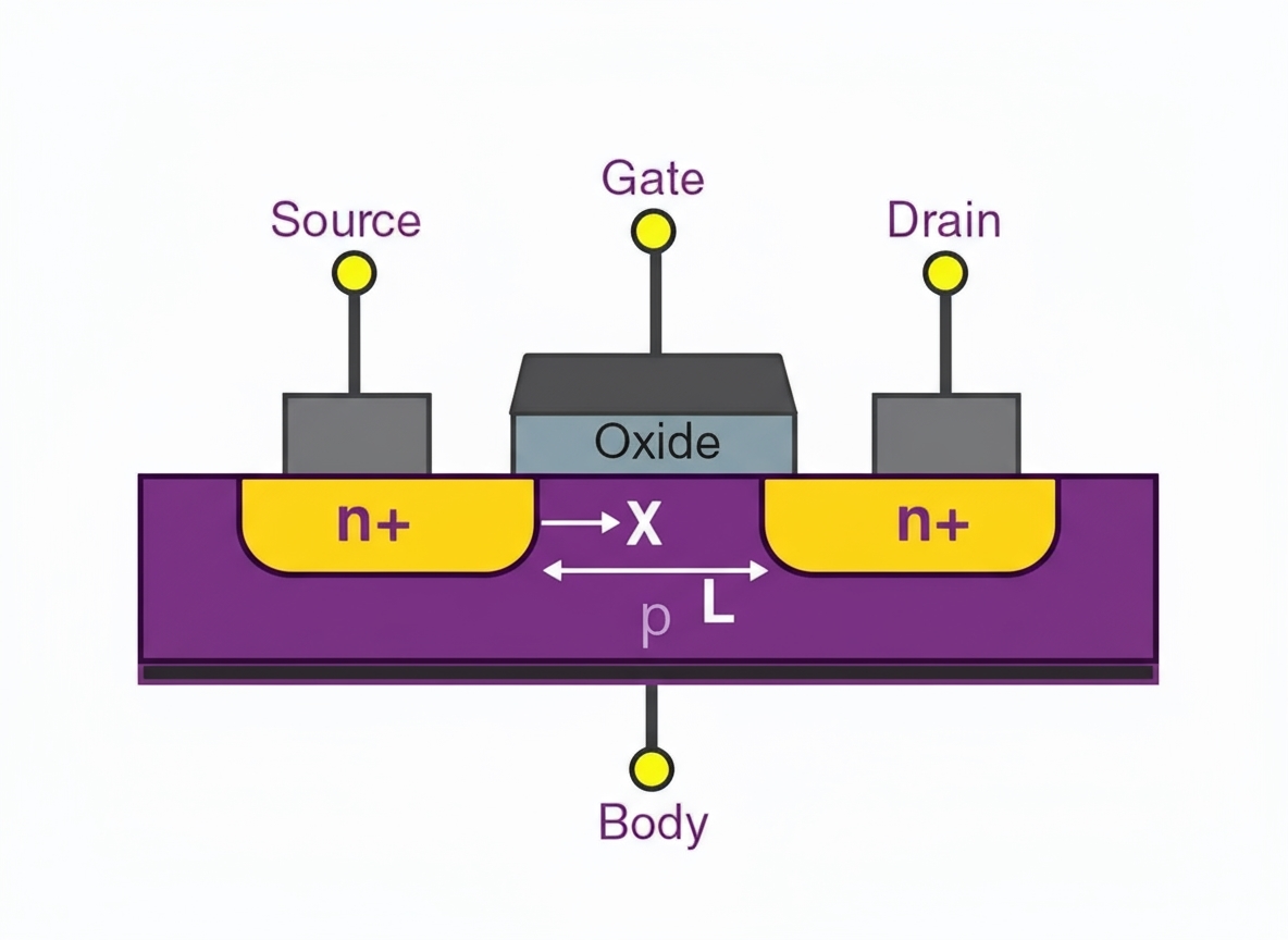
MOSFET-Based Level Conversion
Applicable Scenarios
Suitable for most level conversion applications.
Advantages
- Supports bidirectional signal transmission
- Low conduction voltage drop
- Capable of high-frequency signal transmission
Operational Analysis (I2C Signal Line Example)
For an I2C signal line (e.g., SDA):
- When SDA1 outputs a high signal, the MOSFET¡¯s gate-source voltage (Vgs) is 0V, keeping the MOSFET off, and SDA2 is pulled up to 5V by a resistor.
- When SDA1 outputs a low signal, Vgs equals 3.3V, exceeding the threshold voltage, turning the MOSFET on and pulling SDA2 low.
- When SDA2 outputs a high signal, the MOSFET remains off, and SDA1 is pulled up to 3.3V by a resistor.
- When SDA2 outputs a low signal, the MOSFET¡¯s body diode pulls SDA1 low, and with Vgs approximately 3.3V, the MOSFET conducts, further pulling SDA1 low.
Level Conversion ICs
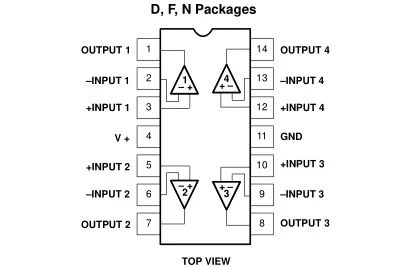
For applications requiring high-frequency signal conversion with minimal voltage drop, dedicated level conversion integrated circuits (ICs) are available. These ICs offer the following features:
- Wide voltage range: 1.65V to 3.6V (side A) and 2.3V to 5.5V (side B)
- Maximum data rate: 50 Mbps
- Multiple package options
- Support for multiple channels (e.g., 4 channels)
- Suitable for protocols such as I2C, UART, and GPIO
Conclusion
Various level conversion methods and circuits are available, each suited to specific requirements. For most applications, dedicated level conversion ICs are recommended due to their maturity, reliability, and versatility.
 ALLPCB


