ALLPCB


Introduction
With the rise of mobile devices and improvements in semiconductor processes, power consumption has become an increasingly important concern in chip design. Increased attention to power can be viewed from two perspectives: end users and chip designers.
User perspective
Portable devices such as smartphones, tablets, and TWS earbuds play important roles in daily life. Higher chip power consumption shortens operating time for a given battery capacity, which can inconvenience activities like travel, payments, and communication. Higher power dissipation also generates more heat; excessive heating raises thermal noise and can affect device operation, slowing performance and degrading the user experience.
Designer perspective
Process advancement increases transistor density and operating speed while interconnects become finer. The on-chip power distribution network must deliver energy to each block with fewer routing resources, so designers must reduce power during the design phase. Poor low-power design can also increase downstream costs: higher heat may require more elaborate packaging and cooling solutions, raising package cost and reducing market competitiveness. Therefore, implementing low-power techniques is necessary.
Sources of power consumption
To design for low power, it is essential to understand the sources of chip power consumption. Broadly, power comes from three sources.
1. Switching power
In digital CMOS circuits, switching power is consumed when charging and discharging load capacitances. For example, in a CMOS inverter: when Vin = 0, the PMOS conducts and the NMOS is off, so VDD charges the load capacitance Cload and Vout goes high; when Vin = 1, the PMOS is off and the NMOS conducts, discharging the load capacitance to ground and Vout goes low. These charge and discharge cycles cause switching power.
2. Short-circuit power
Also called internal power, short-circuit power occurs during input transitions. Transitions are not instantaneous, so there is a period when both PMOS and NMOS are simultaneously on, creating a direct current path from VDD to VSS and producing short-circuit current.
3. Static power
In CMOS circuits, static power is mainly due to leakage current. Leakage has several components:
- PN junction reverse current
- Subthreshold leakage between source and drain
- Gate leakage, including gate-to-drain induced leakage
- Tunneling leakage between gate and substrate
Power control techniques
From the previous section, power consumption is mainly related to supply voltage, operating frequency, and circuit load. Designers use several techniques to address these factors.
1. Clock gating
The clock path typically has the highest toggle rate and can account for 40% or more of total chip power. After the PLL and pre-divider, the clock drives thousands of registers and requires many buffers to maintain drive strength. Each clock cycle toggles all cells in the path. If a subsystem or module is idle but its clock keeps toggling, substantial power is wasted. Clock gating dynamically disables the clock to parts of the design based on system or task requirements, significantly reducing power.
2. DVFS
DVFS (dynamic voltage and frequency scaling) adjusts voltage and frequency according to workload. If a circuit can estimate the required amount of work for a task, the clock frequency can be lowered to the minimum level that still meets timing requirements. Frequency and voltage are closely related; reducing frequency allows lowering the supply voltage, and reducing both results in large power savings.
3. Multi-voltage domains
Dynamic power scales with the square of voltage and static power scales approximately linearly with voltage, so lowering voltage is effective. Multi-voltage design assigns different modules or IP blocks to different voltage domains so each block operates at an appropriate supply level, avoiding the waste of a single global voltage domain.
4. Power gating
When a module or IP block is idle, isolating its clocks and inputs does not eliminate leakage. As transistor counts increase, leakage becomes a larger portion of total power. Power gating turns off the supply to specific regions, placing them into deep sleep with very low leakage.
5. Multi-threshold design
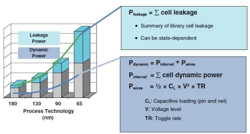
Process scaling increases the proportion of static power. In technologies at 90 nm and below, static power can account for over 20% of total power, necessitating deeper optimizations. Multi-threshold CMOS uses transistors with different threshold voltages to balance performance and leakage.
6. Low-power floorplanning and layout
Layout and floorplanning rules also affect power. Proper placement of power domains, isolation cells, and routing of power nets can reduce leakage, minimize IR drop, and improve the effectiveness of techniques like power gating and multi-voltage domains.