 ALLPCB


Definition
An analog switch is a semiconductor device used to perform signal routing within a signal chain. It uses MOSFETs as switch elements to open or close signal paths. Typical analog switch circuits can achieve high off-state impedance, often in the megaohm range, which is one of their key roles. This article explains the function of analog switches and how to select them.
Operating Principle
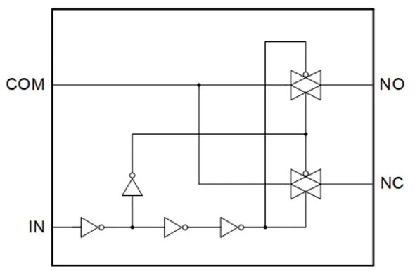
Figure 1. Analog switch operating principle
As shown in Figure 1, when the IN input is low, logic control closes the channel between COM and NC while opening the channel between COM and NO. When IN is high, the states reverse.
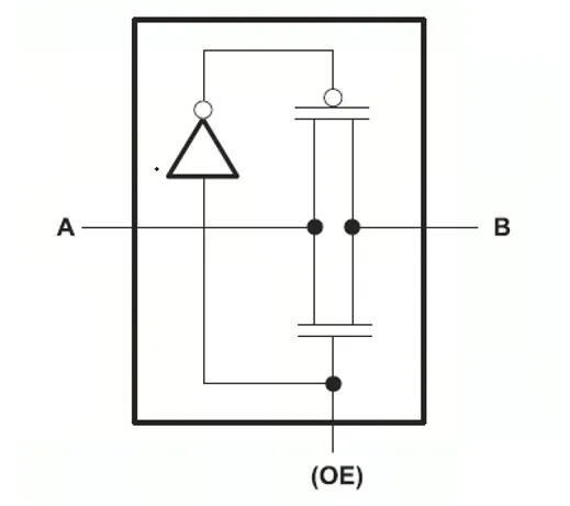
Figure 2. Transmission-gate schematic
Figure 2 shows the FET transmission gate used for NO/NC ports. It consists of an N-channel transistor in parallel with a P-channel transistor. When OE is high, the inverter drives the P-channel and the N-channel into conduction, connecting A to B. When OE is low, both transistors are off and A is disconnected from B.
How to Choose an Analog Switch
Analog switches are commonly used for signal routing in small-signal applications. Compared with mechanical contact switches, integrated electronic switches offer faster switching, no contact bounce, lower power consumption, smaller size, and higher reliability, but they also have limitations such as higher on-resistance, limited input current capacity, and smaller dynamic range. Use integrated analog switches where fast switching and compact system size are priorities. Many analog switches are implemented in CMOS and can cover a wide frequency range.
1. Number of Channels
Integrated analog switches often contain multiple channels. Channel count affects transmission accuracy and switching performance. More channels increase parasitic capacitance. Non-selected channels are not perfect opens but present high impedance and leakage current; coupling and parasitic capacitance between channels can cause crosstalk and interference among channels.
2. Leakage Current
An ideal switch would have zero on-resistance and infinite off-resistance with zero leakage current. In practice, off-state leakage exists; typical CMOS leakage is on the order of 1 nA. If the source impedance is high or the transmitted signal is a current, off-state leakage becomes critical. Lower leakage current is generally preferred in these cases.
3. On-Resistance
On-resistance magnitude and flatness are important. On-resistance causes signal loss and reduces accuracy, especially when the load is low impedance. Choose a switch with sufficiently low on-resistance for the application. Note that on-resistance depends on supply voltage: higher supply voltages generally reduce on-resistance. There is a trade-off between on-resistance and leakage: reducing on-resistance by increasing channel size tends to increase leakage current. On-resistance varies with input voltage; on-resistance flatness is defined as the maximum variation of RON over a specified input voltage range, ΔRON = RONMAX RONMIN. Smaller ΔRON indicates a flatter RON and better performance. Channel-to-channel RON matching affects measurement error when multiple signals are sampled through different channels.
4. Switching Speed
Switching speed is the time to turn on or off, typically given by turn-on time (tON) and turn-off time (tOFF). For rapidly changing signals, choose a switch with sufficiently fast switching. Also ensure compatibility with downstream sample-and-hold circuits and ADC conversion speeds to optimize overall performance and cost.
5. Voltage Rating
Analog switches are typically used in low-voltage electronic systems, with maximum voltage ratings usually within 15 V. Common maximum supply voltages include 3.3 V, 5 V, 12 V, and 15 V. Ensure the maximum signal voltage in the signal chain does not exceed the device rating.
6. THD (Total Harmonic Distortion)
THD measures how well an analog switch preserves audio signals and is important in audio applications. THD is defined as the dB ratio of signal power to harmonic and noise power. THD relates to on-resistance flatness: as on-resistance and its variation with input voltage increase, THD performance typically degrades. Within the specified input voltage range, a flatter on-resistance usually yields better THD.
Applications and Practical Considerations
Unlike mechanical switches, analog switches exhibit semiconductor characteristics that require attention in circuit design.
1. RON Varies with Input Voltage (VIN)
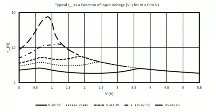
Figure 3. RON versus VIN relationship
2. Charge Injection
For mechanical switches, lower RON is always desirable to minimize loss. For analog switches, very low RON can require larger chip area and result in larger input capacitance, which increases charge and discharge current each switching cycle. The time constant t = RC depends on load resistance R and capacitance C and can last tens of nanoseconds. Low RON can therefore lead to longer effective turn-on and turn-off behavior. Select an analog switch by balancing RON and charge injection.
3. Input Voltage Range and ESD Limits
When the input signal goes below ground or above the supply, MOSFETs can become reverse-biased. If the voltage exceeds specified limits (typically about 0.3 V beyond rails), the switch may malfunction or be damaged. Ensure input signals stay within specified ranges.
Troubleshooting Example: Audio Front-End Routing
Figure 4 shows a front-end amplifier and signal selection circuit for an audio application using a quad op amp and a dual analog switch.
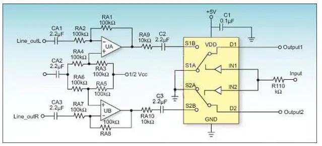
Figure 4. Audio front-end amplification and signal routing
The design intended that when Input = 0, Line_outL and Line_outR are selected, and when Input = 1, Phone_outL and Phone_outR are selected. In testing, when Input = 1 a portion of Line_outL and Line_outR leaked to D1 and D2. Network analysis showed the switch off-state isolation at 10 kHz was 120 dB, so the chip itself appeared to be functioning.
1. Missing DC Bias on the Switch Inputs
The analog switch can be modeled as in Figure 5. CMOS switches typically allow input signals down to around 0.3 V. If the input goes below that threshold, the chip may not operate correctly or may be damaged. In Figure 4 the switch inputs had no DC bias, allowing parts of the input to go negative; the switch therefore did not behave correctly.
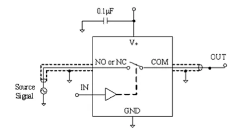
Figure 5. Equivalent circuit of an analog switch
2. Missing Load Resistance at D1 and D2
When the switch is off, its input and output ports present an equivalent series capacitance C. If there is an equivalent resistance R from the switch output to ground, the off-state equivalent circuit is shown in Figure 6.
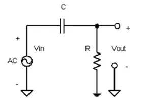
Figure 6. Off-state equivalent circuit of an analog switch
The switch and load form an RC filter, yielding the relation shown in the image below:
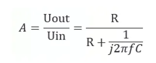
In this expression, Uout is the switch output, Uin is the switch input, R is the load resistance at the switch output, C is the equivalent off-state capacitance, and f is the input frequency.
Because C is designed to be small, at audio frequencies the gain A is determined by R and f. When R is small, frequency dominates and A ? 1, so the signal is effectively isolated. When R is large, R dominates and A → 1, so the signal can leak through. If the output node is floating, the effective resistance to ground tends toward infinity and the off-state isolation is compromised.
Correcting the missing DC bias and adding appropriate coupling or load resistances at the outputs resolved the leakage issue in the audio example. Understanding these basic analog switch concepts is essential for correct application.


