ALLPCB


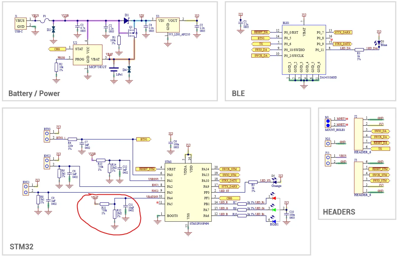
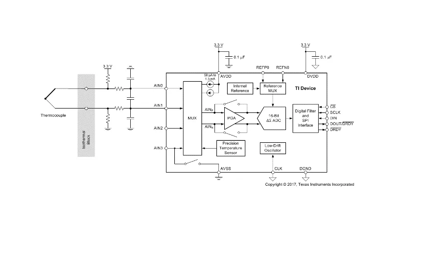
The ADS7863A is a precision 16-bit analog-to-digital converter (ADC) that integrates multiple functions to reduce system cost and component count in small-sensor measurement applications. The device provides two differential or four single-ended inputs, a flexible input multiplexer (MUX), a low-noise programmable gain amplifier (PGA), two programmable excitation current sources, a reference voltage source, an oscillator, a low-side switch, and a precision temperature sensor.
The device supports conversion data rates up to 2000 samples per second (SPS) and features single-cycle settling. At 20 SPS, the digital filter provides simultaneous 50 Hz and 60 Hz rejection for noisy industrial environments. The internal PGA offers gains up to 128 V/V. This PGA makes the ADS1120 well suited for measuring small sensor signals such as resistance temperature detectors (RTDs), thermocouples, thermistors, and bridge sensors. The device supports pseudo-differential or full-differential measurements when the PGA is used. Alternatively, the PGA can be bypassed while still providing high input impedance and gains up to 4 V/V for single-ended measurements.
When operating in duty-cycle mode with the PGA disabled, supply current can be as low as 120 μA. The ADS1120 is available in a pinless VQFN-16 or TSSOP-16 package and is specified for –40°C to +125°C.
Features
- Low current consumption: as low as 120 μA in duty-cycle mode (typical)
- Wide supply range: 2.3 V to 5.5 V
- Programmable gain: 1 V/V to 128 V/V
- Programmable data rate: up to 2 kSPS
- 16-bit noise-free resolution at 20 SPS
- Simultaneous 50 Hz and 60 Hz rejection at 20 SPS using a single-cycle-settling digital filter
- Two differential or four single-ended inputs
- Dual matched programmable current sources: 50 μA to 1.5 mA
- Internal 2.048 V reference: 5 ppm/°C (typical) drift
- Internal 2% accurate oscillator
- Internal temperature sensor: 0.5°C (typical) accuracy
- SPI-compatible interface (Mode 1)
- Package: 3.5 mm × 3.5 mm × 0.9 mm VQFN
Block diagram
The ADS7863A is a Texas Instruments dual-channel 12-bit high-speed ADC. Its core advantages are synchronous sampling, strong interference rejection, and flexible power and operating modes. It is designed for industrial high-speed signal acquisition scenarios such as motor control, multi-axis positioning systems, and three-phase power control.
1. Core product parameters
1. Basic specifications
- Resolution and sampling: 12-bit no-miss resolution, synchronized dual-ADC architecture, up to 2 MSPS; conversion time down to 406.25 ns (32 MHz clock), acquisition time 62.5 ns
- Package and temperature: 24-pin SSOP (DBQ) or 4 mm × 4 mm QFN (RGE) package; operating temperature –40°C to 125°C, maximum junction temperature 150°C
- Power and consumption: analog supply (AVDD) 2.7 V–5.5 V, digital supply (BVDD) 2.7 V–5.5 V; typical power 45 mW at 5 V, deep-power-down mode 1 μA
- Input characteristics: 4 fully differential or 6 pseudo-differential inputs (two channel groups); input capacitance 2 pF (single-ended)/4 pF (differential), leakage current ±1 nA; full-scale input range ±VREF (VREF typical 2.5 V)
2. Performance characteristics
- Dynamic metrics: at 100 kHz input, SNR typical 71.5 dB, THD typical ?81 dB, SFDR typical 84 dB, common-mode rejection ratio (CMRR) 72 dB (100 kHz)
- Static accuracy: integral nonlinearity (INL) ±0.5 LSB (?40°C to 85°C), differential nonlinearity (DNL) ±0.5 LSB; input offset error ±0.5 LSB, offset drift ±3 μV/°C; gain error ±0.1%, gain drift ±1 ppm/°C
- Reference source: internal 2.5 V programmable reference via a 10-bit DAC with 2.44 mV steps; reference drift ±10 ppm/°C, output current ±2 mA; supports external reference input (0.5 V–2.525 V)
- Reliability: ESD protection (HBM ±4 kV, CDM ±1.5 kV); power-supply rejection ratio (PSRR) 70 dB, suitable for noisy industrial power environments
3. Key functional parameters
- Operating modes: supports four main operating modes (M0/M1 pin configuration), including manual/automatic channel selection and single/dual output modes; supports pseudo-differential input mode for flexible channel expansion
- Power management: three power-down modes (deep power-down, NAP, automatic NAP) to reduce power as needed; automatic NAP enters sleep after mode transition and has short wake-up time
- Interface features: SPI-compatible serial interface, dual outputs (SDOA/SDOB), supports 12-bit two's complement output; SDI pin can be used to configure channel selection, reference voltage, and power-down mode
2. Key functional features
1. High-speed synchronous sampling
- Synchronized dual architecture: two ADCs sample simultaneously to ensure phase alignment across channels, suitable for synchronized three-phase current/voltage acquisition
- Robust interference rejection: fully differential input architecture with CMRR of 72 dB at 100 kHz, effectively suppresses industrial common-mode noise; series 200 Ω input resistors reduce the impact of sampling capacitance on driving circuitry
- Flexible input configuration: supports two fully differential inputs (two channels per group) or three pseudo-differential inputs (three channels per group); channel selection via SDI register to match different sensor signal types
2. Flexible configuration and power optimization
- Programmable reference: internal 2.5 V reference adjustable via a 10-bit DAC, eliminating external components for many input ranges; supports external reference for high-accuracy calibration
- Multiple power-down modes: deep power-down mode consumes 1 μA, NAP mode enables 200 ns fast sleep/wake, automatic NAP suits periodic sampling, balancing speed and power
- Backward compatibility: SSOP package pin-compatible with ADS7861/ADS8361, enabling direct replacements while preserving existing hardware layouts
3. Industrial reliability
- Wide voltage compatibility: separate analog and digital supplies with wide ranges to support various regulated supplies in industrial systems
- Interference immunity: digital inputs include Schmitt triggers; supply pins should be decoupled locally to enhance EMI immunity; clock supports 1 MHz–32 MHz, duty cycle compatible with 30%–70%
- Fault protection: reference output short-circuit current limit 50 mA, input voltage tolerance ±0.3 V beyond supply rails to improve system robustness
3. Typical applications
- Industrial control: current/voltage synchronous acquisition in motor control, servo position feedback conversion
- Power electronics: three-phase inverters and variable-frequency drives for voltage/current sensing and power quality monitoring
- Motion control: multi-axis robots and CNC machines requiring synchronized multi-channel position/velocity acquisition
- Test and measurement: high-speed data acquisition systems and portable instruments for multi-channel signal capture
4. Design and usage recommendations
1. Interface and configuration
- Mode selection: select automatic channel mode (M0=1) for multi-channel synchronized sampling; select manual mode (M0=0) for single-channel high-speed sampling. For dual outputs choose SDOA+SDOB (M1=0); for pin savings choose single output (M1=1).
- Reference configuration: prefer the internal programmable reference; place a ≥470 nF ceramic capacitor at the REFIN pin for stability. External references must have sufficient drive capability to avoid oscillation.
- Channel configuration: use full-differential mode in high-interference environments; pseudo-differential expands channel count. Switch channels via C1/C0 bits in the SDI register.
2. Power supply and PCB layout
- Power design: decouple AVDD and BVDD locally with 0.1 μF ceramic plus 1 μF electrolytic capacitor; connect analog ground (AGND) and digital ground (BGND) at a single point with voltage difference under 0.3 V.
- Layout guidelines: separate analog inputs from digital signals. Keep clock traces short and away from analog channels. Keep reference routing low impedance (≤10 Ω) and avoid placing it near switch-mode supplies or power components.
- Input driving: for high-speed acquisition, use buffer amplifiers with bandwidth ≥23 MHz (for example OPA365) to meet sampling capacitor charging requirements; add series input resistors to balance bandwidth and noise.
3. Optimization and calibration
- Timing optimization: CONVST and RD can be tied together to simplify control. CONVST high time should be ≥20 ns. Ensure clock stability to avoid jitter-related accuracy loss.
- Calibration recommendations: use the SDI register to adjust the internal reference DAC for gain calibration. In multi-channel systems, use offset and gain matching to reduce channel-to-channel errors.
- Power optimization: enable automatic NAP mode for sub-full-speed scenarios and switch to deep power-down for long idle periods to reduce system power consumption.