ALLPCB


Introduction
In electronic design, high-precision analog-to-digital converters (ADCs) are key components for accurate data acquisition. TI's ADS1240 and ADS1241 are 24-bit ADCs that combine high resolution and extensive features. They are commonly used in industrial process control, weighing scales, chromatography, and other applications. This article analyzes the characteristics, operating principles, and application examples of these converters to provide engineers with a technical reference.
1. Product overview
The ADS1240 and ADS1241 are 24-bit, high-precision, wide-dynamic-range delta-sigma ADCs. They operate from 2.7 V to 5.25 V and include the following notable features:
- High-precision conversion: Up to 24-bit no-missing-codes performance, with effective resolution up to 21 bits (PGA = 1) and 19 bits (PGA = 128). Integral nonlinearity is typically ±0.0015%.
- Mains interference rejection: Simultaneous suppression of 50 Hz and 60 Hz interference, with rejection ratios down to -90 dB in challenging electromagnetic environments.
- Programmable gain amplifier (PGA): Gain settings from 1 to 128 allow flexible scaling of input signal amplitude to improve conversion precision.
- Single-cycle settling: A single-cycle-settling digital filter provides valid data on the first conversion after a channel switch.
- Multiple functional features: On-chip calibration, SPI-compatible interface, up to eight input channels and data I/O pins, and sensor-fault detection.
2. Key features, detailed
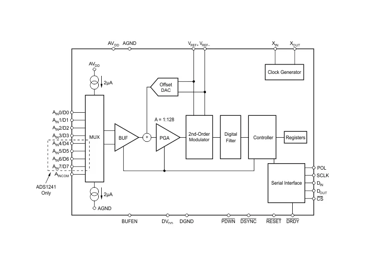
2.1 Input multiplexer
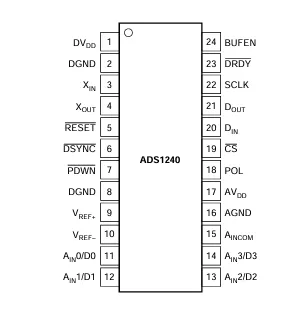
The input multiplexer allows selection of arbitrary combinations of differential inputs on any channel. The ADS1241 supports up to eight single-ended inputs or four independent differential inputs. The ADS1240 supports up to four single-ended inputs or two independent differential inputs. To minimize settling error, synchronize multiplexer switching with the DRDY falling edge.
2.2 Fault-detection current sources
Enabling the BOCS bit in the SETUP register activates two 2 μA fault-detection current sources connected to the positive and negative inputs. When a sensor is open, the positive input current source pulls the positive input toward the positive analog supply and the negative input current source pulls the negative input to ground, causing the converter to output full-scale. When a sensor is shorted, the inputs are at the same potential and the converter output is approximately zero.
2.3 Input buffers
For systems requiring high input impedance, the ADS1240/41 provide chopper-stabilized differential FET input voltage buffers. When enabled, input impedance increases to approximately 5 GΩ. The buffer input range is roughly 50 mV to AV_DD - 1.5 V; linearity degrades outside this range. The buffer is enabled via the BUFEN pin or the BUFEN bit in the ACR register, and it consumes additional current depending on the PGA setting when enabled.
2.4 Programmable gain amplifier (PGA)
The PGA supports gains of 1, 2, 4, 8, 16, 32, 64, or 128. Using the PGA increases effective ADC resolution. For example, with a 5 V full-scale input and PGA = 1, the resolution can be as fine as 1 μV; with PGA = 128 and a 39 mV full-scale input, the resolution can be as fine as 75 nV. Note that AV_DD current increases when PGA is set above 4.
2.5 Offset DAC (ODAC)
The offset DAC (ODAC) register allows shifting the PGA input offset by up to half the full-scale input range. The ODAC register is an 8-bit value where the MSB is a sign bit and the remaining 7 bits set the offset magnitude. Using the offset DAC does not reduce ADC performance.
2.6 Modulator
The modulator is a single-loop second-order system. The modulator clock speed f_MOD is derived from the external clock f_OSC by a divider controlled by the SPEED bits in the SETUP register.
2.7 Calibration
The ADS1240 and ADS1241 support two calibration modes: self-calibration and system calibration. Self-calibration commands SELFGCAL, SELFOCAL, and SELFCAL perform gain calibration, offset calibration, and both, respectively. System calibration commands SYSOCAL and SYSGCAL correct internal and external offset and gain errors. Calibration should be performed after power-up, on significant temperature changes, or after changing the PGA. ODAC must be disabled during calibration. After calibration completes, DRDY goes low; the first conversion result after calibration should be discarded.
2.8 External voltage reference
These devices require an external differential voltage reference. The reference voltage is the potential difference between the +VREF and -VREF pins. The absolute voltage at each pin must remain between AGND and AV_DD. Allowed reference voltage ranges depend on AV_DD and the RANGE bits in the ACR register.
2.9 Clock generator
The clock source may be a crystal, an oscillator, or an external clock. When using a crystal, external capacitors are required to ensure startup and stable frequency. XOUT is for the external crystal only and must not be used to drive external circuitry.
2.10 Digital filter
The devices use a 1279-tap linear-phase finite impulse response (FIR) digital filter that supports programmable output data rates. With a 2.4576 MHz crystal, output data rates of 15 Hz, 7.5 Hz, or 3.75 Hz are available; at these settings the digital filter suppresses both 50 Hz and 60 Hz interference. Using different crystal frequencies changes the available data rates and the interference suppression frequencies.
2.11 Data I/O pins
The ADS1240 provides four dual-purpose pins and the ADS1241 provides eight, which serve both as analog inputs and data I/O. These pins are powered by AV_DD and are configurable via the IOCON, DIR, and DIO registers.
2.12 Serial peripheral interface (SPI)
The devices use a standard four-wire SPI interface: CS, SCLK, DIN, and DOUT. Two serial clock polarities are supported via the POL pin. CS must be driven low externally before communication and held low during the transaction. SCLK is a Schmitt-trigger input that clocks DIN and DOUT. The POL pin sets whether data is clocked on the rising or falling SCLK edge.
2.13 Data-ready (DRDY) pin
The DRDY line indicates status. DRDY goes low when the internal data register contains new data. Reading the data resets DRDY high. DRDY also goes high before the output register updates, indicating that data should not be read at that time. The DRDY status is also available by reading bit 7 of the ACR register.
2.14 DSYNC operation
Synchronization can be performed using the DSYNC pin or the DSYNC command. On a DSYNC pin falling edge, digital circuitry is reset and the serial interface is disabled while DSYNC is low. When DSYNC returns high, synchronization occurs on the next system clock rising edge. When sending the DSYNC command, the digital filter resets on the last SCLK edge of the command; the modulator remains in reset until the next SCLK edge, and synchronization then occurs on the next system clock rising edge.
2.15 Power-up ramp rate
The power-on reset circuit supports a digital supply ramp rate as low as 1 V per 10 ms. To ensure normal operation, the supply should ramp monotonically.
2.16 Reset
Registers can be returned to default values by asserting the RESET pin, by sending the RESET command, or by applying a specific waveform on SCLK.
3. Registers and control commands
3.1 Registers
The ADS1240 and ADS1241 are configured via 16 registers, including SETUP, MUX, ACR, and ODAC. Individual bits in these registers control various functions such as PGA gain selection, input channel selection, data format, and clock speed.
3.2 Control commands
A set of control commands manage converter operations, including reading data (RDATA, RDATAC), stopping continuous read (STOPC), reading and writing registers (RREG, WREG), calibration (SELFCAL, SELFOCAL, SYSOCAL, SYSGCAL), and power-state control (WAKEUP, SLEEP).
4. Application examples
4.1 General weighing scale
In a general weighing scale application, set the internal PGA to 64 or 128 depending on the sensor's maximum output voltage, and connect the load cell output directly to the ADS1240 differential input.
4.2 High-precision weighing scale
In high-precision weighing applications, a front-end differential amplifier can help maximize dynamic range and improve measurement accuracy.
5. Conclusion
The ADS1240 and ADS1241 offer high resolution, comprehensive features, and flexible configuration, making them suitable for precision data acquisition and processing applications. Understanding their operating principles, register configuration, and control commands enables engineers to design efficient and stable systems. Attention to power management, clock stability, and electromagnetic compatibility is important to ensure system performance and reliability.