ALLPCB


The ADS1131 is an 18-bit, high-precision analog-to-digital converter (ADC) designed as a complete front end for bridge sensors such as load cells, strain gauges, and weighing scales. It integrates a low-noise programmable gain amplifier (PGA), an internal oscillator, a precision 18-bit delta-sigma ADC, and a low-side bridge power switch. Data is output over a simple, easily isolated serial interface suitable for connection to MSP430 and other microcontrollers.
Overview
The low-noise amplifier has a fixed gain of 64 and supports a differential full-scale input of +/-39 mV with a 5 V reference and +/-23.4 mV with a 3 V reference. The delta-sigma ADC provides 18-bit effective resolution using a third-order modulator and a fourth-order digital filter. Two data rates are available: 10 SPS (with 50 Hz and 60 Hz rejection) and 80 SPS. The device supports a low-power standby mode and a power-down mode.
Control is via dedicated pins; there are no programmable digital registers. The converter is available in a 16-pin SOIC package and operates over a -40 C to +85 C range.
Key Features
- Complete front-end for bridge sensors.
- 16-pin SOIC package.
- Integrated low-noise amplifier, gain 64.
- Internal oscillator.
- Low-side bridge power switch for sensor supply.
- 18-bit noise-free resolution.
- Selectable 10 SPS or 80 SPS data rates.
- Simultaneous 50 Hz and 60 Hz rejection in 10 SPS mode.
- External voltage reference up to 5 V for ratiometric measurements.
- Simple pin-driven control.
- Two-wire serial digital interface.
- Supply range: 3 V to 5.3 V.
- Operating temperature: -40 C to +85 C.
Block Diagram
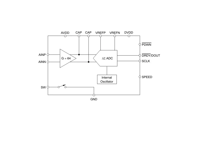
The ADS1131 is a Texas Instruments (TI) 18-bit ADC that integrates a low-noise PGA, a bridge sensor power switch, and a mains-frequency-rejecting digital filter. It supports selectable sampling rates of 10 SPS and 80 SPS and is intended for bridge-sensor signal acquisition in applications such as weighing scales and strain measurement. The device operates over -40 C to +85 C and provides a compact front-end solution for bridge sensors.
1. Core Product Parameters
1.1 Resolution and Sampling
- 18-bit noise-free resolution. Sampling rate selected via the SPEED pin (10 SPS or 80 SPS). The 10 SPS mode provides simultaneous 50 Hz and 60 Hz rejection. The 80 SPS mode is suitable for faster measurement needs.
1.2 Input and Gain
- Integrated fixed-gain low-noise amplifier with gain of 64. Differential full-scale inputs: +/-39 mV with 5 V reference, +/-23.4 mV with 3 V reference.
- Common-mode input range: 1.5 V to AVDD - 1.5 V. Differential input current +/-2 nA. Input protection diodes clamp signals to prevent overvoltage damage.
1.3 Accuracy
- Integral nonlinearity (INL) +/-8 ppm. Input offset error 10 uV. Offset drift +/-15 nV/C. Gain error +/-1% FSR. Gain drift +/-4 ppm/C.
- Common-mode rejection ratio (CMRR) 110 dB (DC). Power-supply rejection ratio (PSRR) 100 dB (DC).
1.4 Noise
- Peak-to-peak noise: 300 nV in 10 SPS mode, 500 nV in 80 SPS mode. Noise-equivalent resolution is high, suitable for low-level signal acquisition.
1.5 Environmental and Packaging
- Operating temperature: -40 C to +85 C.
- Package: 16-pin SOIC (D), RoHS compliant. MSL level 2, peak reflow temperature 260 C.
- ESD protection: observe standard electrostatic discharge precautions during handling.
- Power consumption: active mode approx. 5 mW at 5 V and 2.9 mW at 3 V. Standby/power-down current as low as 0.1 uA.
2. Key Functional Features
2.1 Sensor Interface and Power
- Bridge sensor support: integrated low-side power switch (SW pin). The switch closes to power the sensor during conversions and opens in standby/power-down to reduce power consumption. Typical on-resistance 3.5 ohm (typical, 5 V / 30 mA), suitable for a wide range of bridge sensors.
- Reference input: external reference supported (1.5 V to AVDD + 0.1 V). Reference input current 10 nA, enabling ratiometric measurements and improved accuracy.
2.2 Signal Processing and Filtering
- Digital filtering: 4th-order sinc filter. 10 SPS mode -3 dB cutoff 3.32 Hz; 80 SPS mode cutoff 11.64 Hz. The filter provides frequency notch characteristics to suppress mains interference without additional hardware filtering.
- Settling: after a step change to the input, settling requires 4 conversion cycles. When doing continuous measurements, discard the first 4 readings after a step to ensure accuracy.
2.3 Control and Communication
- Pin control only, no register configuration. SPEED selects sample rate, PDWN controls power-down. Standby mode is entered by holding SCLK high; power-down mode is entered by pulling PDWN low.
- Data interface: two-wire serial interface using SCLK and DRDY/DOUT. The DRDY/DOUT pin indicates data-ready and provides data output. Output format is 18-bit two's complement, MSB first. Maximum SCLK frequency 5 MHz.
3. Applications and Design Considerations
3.1 Typical Applications
- Weighing and force measurement: electronic scales and industrial weighing sensors.
- Strain and pressure sensing: strain gauges and pressure sensor signal conversion.
- Industrial control: low-level analog signal acquisition in process control.
3.2 Hardware Design Recommendations
- External components: connect a 0.1 uF NPO/C0G capacitor to the CAP pin to form a low-pass filter with internal resistance (cutoff ~720 Hz). Place this capacitor close to the pin. Add 0.1 uF decoupling capacitors at AVDD and DVDD to reduce supply noise.
- Input configuration: for differential inputs, use AINP and AINN. For single-ended input, tie AINN to ground. Use a low-noise reference source for the reference input. Keep VREFP/VREFN pins away from digital noise sources.
- Grounding and layout: connect analog and digital grounds at a single point. Separate sensor signal routing from digital lines. Connect the SW pin directly to the sensor ground end to improve common-mode rejection.
3.3 Software and Configuration
- Sampling rate selection: choose 10 SPS in environments with strong mains interference, and 80 SPS where faster response is required.
- Data reading: DRDY/DOUT pulled low indicates data ready. Data is clocked out on SCLK rising edges (18 bits). The 19th SCLK can be used to force the pin high for polling convenience.
- Mode switching: the first sample after standby is valid immediately. After waking from power-down, allow 7.95 us for stabilization before reading data.
4. Selection Guidance
- Advantages: integrates PGA, sensor power switch, and mains-rejecting filter, minimizing external components and simplifying bridge sensor front-end design. Low noise and high CMRR make it suitable for low-level signal acquisition. Pin-based control eliminates the need for register programming and simplifies development.
- Recommended use: designed specifically for bridge sensors and suitable for weighing, strain, and pressure measurement where high-precision, low-level signal acquisition is required. Use with a low-noise reference to fully achieve the device's accuracy potential.