 ALLPCB


In the fast-evolving world of electronics, the demand for smaller, faster, and more powerful devices is relentless. High-Density Interconnect (HDI) multilayer PCBs are at the heart of this revolution, enabling compact designs with superior performance. If you're looking to understand HDI multilayer PCB design rules, the role of microvias in HDI PCBs, the precision of laser drilling for HDI PCBs, a detailed cost analysis of HDI multilayer PCBs, or the reliability of HDI PCBs, you're in the right place. This comprehensive guide will break down everything you need to know about HDI technology and how it can elevate your next project.
At ALLPCB, we specialize in providing cutting-edge solutions for advanced circuit board designs. Let's dive deep into the world of HDI multilayer PCBs and explore how they unlock new levels of density and functionality for modern electronics.
What Are HDI Multilayer PCBs?
High-Density Interconnect (HDI) multilayer PCBs are advanced circuit boards designed to pack more functionality into a smaller footprint. Unlike traditional PCBs, HDI boards feature finer lines, smaller vias, and higher connection pad density. This allows for more components to be placed on both sides of the board, making them ideal for compact devices like smartphones, wearables, and medical equipment.
The defining characteristic of HDI PCBs is their use of microvias—tiny holes with diameters often less than 150 micrometers (μm)—to connect layers. These microvias, combined with multiple layers (sometimes 8 or more), create a dense network of interconnections that traditional drilling methods can't achieve. The result is a board that supports high-speed signals, often exceeding 5 GHz in applications like 5G devices, while maintaining a slim profile.
Suggested Image Placement: Insert an image here showing a cross-section of an HDI multilayer PCB with labeled microvias and layers. ALT Text: "Cross-section of HDI multilayer PCB showing microvias and dense layers."
Key Benefits of HDI Multilayer PCBs
HDI technology offers several advantages over conventional PCBs, making it a go-to choice for high-performance applications:
- Compact Size: HDI boards reduce the need for larger boards by increasing component density, often shrinking device size by 30-40%.
- Improved Signal Integrity: Shorter interconnects and finer traces (as small as 50 μm) minimize signal loss, supporting frequencies up to 10 GHz in some designs.
- Enhanced Reliability: With precise manufacturing techniques, HDI PCBs offer better thermal management and structural integrity.
- Versatility: Suitable for complex applications in industries like automotive, aerospace, and consumer electronics.
Now that we’ve covered the basics, let’s explore the critical aspects of designing and manufacturing HDI multilayer PCBs, starting with the design rules that ensure success.
HDI Multilayer PCB Design Rules: Building for Success
Designing an HDI multilayer PCB requires careful attention to detail to balance density, performance, and manufacturability. Here are some essential HDI multilayer PCB design rules to follow:
1. Trace Width and Spacing
For HDI boards, trace widths and spacing are often reduced to 75 μm or less to accommodate higher density. However, this must align with the current-carrying capacity and impedance requirements of your circuit. For example, a 50-ohm impedance line for high-speed signals might require a trace width of 60 μm on a specific dielectric material with a thickness of 100 μm.
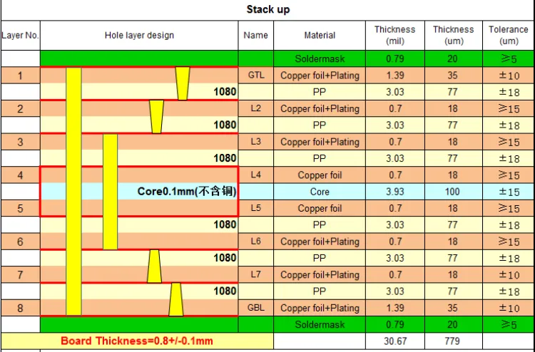
2. Via Types and Placement
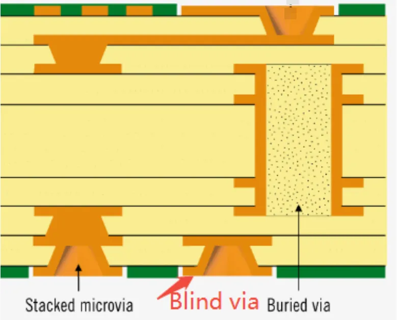
HDI designs often use blind and buried vias alongside microvias to connect layers without consuming surface space. Blind vias connect an outer layer to an inner layer, while buried vias connect only internal layers. Ensure via placement avoids signal interference, and keep microvia aspect ratios (depth-to-diameter) below 1:1 to prevent manufacturing defects.
3. Layer Stack-Up Planning
A typical HDI PCB might have a stack-up of 8-12 layers, with alternating signal and ground planes to reduce electromagnetic interference (EMI). Plan the stack-up early to optimize signal integrity and power distribution. For instance, placing a ground plane adjacent to a high-speed signal layer can reduce crosstalk by up to 20%.
4. Design for Manufacturability (DFM)
Work closely with your manufacturer to ensure your design meets fabrication capabilities. For example, some facilities may have a minimum microvia diameter of 100 μm due to equipment limitations. Following DFM guidelines can reduce production errors and lower costs by 15-25%.
Microvias in HDI PCBs: The Backbone of Density
Microvias in HDI PCBs are small-diameter vias, typically less than 150 μm, that enable high-density connections between layers. Unlike traditional through-hole vias, microvias are created using advanced techniques like laser drilling, allowing for precise placement in tight spaces.
Why Microvias Matter
Microvias allow designers to place more connections in a smaller area, often increasing via density by 50% or more compared to standard vias. This is critical for applications like system-in-package (SiP) designs, where hundreds of connections must fit into a space smaller than 10 mm2. Additionally, microvias reduce parasitic capacitance and inductance, improving signal speeds for applications operating at 3 GHz or higher.
Types of Microvias
- Blind Microvias: Connect the surface layer to an inner layer, often used for surface-mounted components.
- Buried Microvias: Connect internal layers without reaching the surface, saving space on outer layers.
- Stacked Microvias: Multiple microvias stacked on top of each other to connect several layers, common in 10+ layer boards.
While microvias are powerful, they must be designed with care. Overloading a design with stacked microvias can lead to reliability issues if the aspect ratio exceeds 1:1, as deeper holes are harder to plate uniformly.
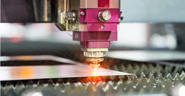
Laser Drilling for HDI PCBs: Precision at Its Best
Laser drilling for HDI PCBs is the preferred method for creating microvias due to its precision and ability to handle small diameters. Unlike mechanical drilling, which struggles with holes smaller than 200 μm, laser drilling can achieve diameters as small as 50 μm with tolerances of ±10 μm.
How Laser Drilling Works
Laser drilling uses a focused beam of light to ablate material, creating clean, precise holes in the PCB substrate. The process is non-contact, reducing the risk of mechanical stress on delicate multilayer boards. Modern systems can drill up to 9,000 vias per second, making it efficient for high-volume production.
Advantages of Laser Drilling
- Accuracy: Achieves microvia diameters below 100 μm with consistent quality.
- Flexibility: Can drill through various materials, including copper and dielectric layers.
- Speed: High drilling rates reduce manufacturing time, often by 20-30% compared to mechanical methods.
However, laser drilling requires specialized equipment and skilled operators, which can impact costs. Balancing precision with budget constraints is key when planning HDI designs.
Cost Analysis of HDI Multilayer PCBs: What to Expect
A thorough cost analysis of HDI multilayer PCBs is essential for budgeting and project planning. While HDI boards offer unmatched performance, they come at a higher price than standard PCBs due to their complexity and advanced manufacturing processes.
Factors Influencing HDI PCB Costs
- Layer Count: An 8-layer HDI board may cost 2-3 times more than a 4-layer standard PCB due to additional materials and processing steps.
- Microvia Density: High-density designs with thousands of microvias increase drilling and plating costs. For example, a design with 5,000 laser-drilled vias could add 10-15% to the total cost.
- Material Selection: High-frequency materials like Rogers or Isola, often used in HDI designs for signal integrity, can cost 20-50% more than standard FR-4.
- Manufacturing Complexity: Techniques like sequential lamination for stacked microvias or fine-line etching add labor and equipment costs.
Cost-Saving Tips
To manage expenses, consider optimizing your design for fewer layers where possible, or using a hybrid approach with HDI only in critical areas. Additionally, partnering with a manufacturer that offers design feedback can reduce iterations and save up to 10% on prototyping costs.
On average, HDI multilayer PCBs can range from $50 to $500 per square foot, depending on complexity, compared to $10-$50 for standard boards. While the upfront cost is higher, the benefits of reduced device size and improved performance often justify the investment for high-end applications.
Reliability of HDI PCBs: Ensuring Long-Term Performance
The reliability of HDI PCBs is a critical consideration, especially for applications in harsh environments like automotive or aerospace. With proper design and manufacturing, HDI boards can achieve exceptional durability and performance.
Factors Affecting Reliability
- Thermal Management: HDI PCBs often handle high power densities, so incorporating thermal vias and heat sinks is essential to prevent failures. For instance, thermal vias can reduce operating temperatures by 10-15°C in high-power designs.
- Microvia Integrity: Poorly plated or overstressed microvias can crack under thermal cycling. Maintaining an aspect ratio below 1:1 and using reliable plating processes can improve lifespan by 30%.
- Material Quality: High-quality dielectrics with low coefficients of thermal expansion (CTE) reduce stress on vias and traces during temperature changes.
Testing for Reliability
Manufacturers often perform rigorous testing, including thermal cycling (from -40°C to 125°C for 1,000 cycles) and microsection analysis, to ensure HDI boards meet industry standards like IPC-6012. These tests confirm that the board can withstand real-world conditions without delamination or via failure.
By focusing on design best practices and partnering with experienced manufacturers, you can achieve HDI PCBs with failure rates as low as 0.1% over a 10-year lifespan, even in demanding applications.
Applications of HDI Multilayer PCBs
HDI technology is transforming industries by enabling compact, high-performance electronics. Here are some key areas where HDI multilayer PCBs shine:
- Consumer Electronics: Smartphones and tablets rely on HDI for slim designs with high-speed processors, often using 6-10 layer boards.
- Automotive: Advanced driver-assistance systems (ADAS) use HDI PCBs for reliable, high-density connections in compact modules.
- Medical Devices: Wearable health monitors and implantable devices benefit from the small size and reliability of HDI technology.
- Telecommunications: 5G infrastructure demands HDI boards to handle frequencies above 6 GHz with minimal signal loss.
Conclusion: Why Choose HDI Multilayer PCBs with ALLPCB?
High-Density Interconnect (HDI) multilayer PCBs are unlocking new possibilities for compact, high-performance electronics. By understanding HDI multilayer PCB design rules, leveraging microvias in HDI PCBs, utilizing laser drilling for HDI PCBs, conducting a thorough cost analysis of HDI multilayer PCBs, and ensuring the reliability of HDI PCBs, you can create cutting-edge designs that meet the demands of modern technology.
At ALLPCB, we’re committed to supporting your innovation with advanced HDI solutions. Whether you’re designing for consumer gadgets or industrial systems, our expertise and state-of-the-art manufacturing capabilities ensure your projects succeed. Ready to unlock the full potential of density in your designs? Let’s bring your ideas to life with precision and reliability.


