 ALLPCB


In the fast-evolving world of automotive electronics, the design of Electronic Control Unit (ECU) PCBs plays a critical role in ensuring vehicle safety, efficiency, and performance. A key aspect of ECU PCB design is the layer stackup, which directly impacts signal integrity, power distribution, and overall reliability. So, what is the ideal layer stackup for optimal ECU PCB performance? Simply put, it’s a carefully planned arrangement of conductive and insulating layers tailored to meet the specific electrical and thermal demands of automotive applications, often involving 4 to 8 layers for most ECUs, with dedicated planes for power and ground to minimize noise and ensure impedance control.
In this comprehensive guide, we’ll dive deep into the nuances of ECU PCB layer stackup design, explore automotive PCB impedance control, and discuss critical factors like signal and power integrity, as well as material selection. Whether you’re an engineer designing automotive electronics or a procurement specialist seeking reliable PCB solutions, this blog will provide actionable insights to enhance your ECU designs.
What Is ECU PCB Layer Stackup Design?
ECU PCB layer stackup design refers to the arrangement of copper layers and insulating materials (dielectrics) in a printed circuit board used in automotive control units. These units manage critical vehicle functions like engine control, braking systems, and infotainment. The stackup defines how many layers the PCB will have, what each layer’s purpose is (e.g., signal, power, or ground), and how they are separated to prevent interference and ensure performance.
A typical ECU PCB might have 4, 6, or 8 layers, depending on the complexity of the system. For instance, a 4-layer stackup might include two signal layers on the top and bottom, with internal power and ground planes to shield signals from electromagnetic interference (EMI). The goal of a well-designed stackup is to optimize signal integrity, manage power distribution, and meet the stringent reliability standards of automotive environments, where temperatures can range from -40°C to 125°C and vibrations are constant.
Why Layer Stackup Matters for ECU Performance
The layer stackup is the backbone of any ECU PCB. A poorly designed stackup can lead to signal crosstalk, power supply noise, or even complete system failure—issues that are unacceptable in automotive applications where safety is paramount. Here’s why stackup design is so critical:
- Signal Integrity: High-speed signals in ECUs, such as those for CAN bus communication (up to 1 Mbps for CAN 2.0 and 5 Mbps for CAN FD), require controlled impedance to prevent signal distortion. A proper stackup ensures that signal traces are routed near ground planes to maintain consistent impedance, often targeting values like 50 ohms for single-ended traces or 90 ohms for differential pairs.
- Power Integrity: ECUs often handle multiple voltage levels (e.g., 3.3V for microcontrollers and 12V for actuators). Dedicated power planes in the stackup reduce voltage drops and noise, ensuring stable operation.
- EMI Reduction: Automotive environments are rife with EMI from motors, switches, and other electronics. A well-designed stackup with ground planes adjacent to signal layers minimizes EMI by providing a return path for currents and shielding sensitive signals.
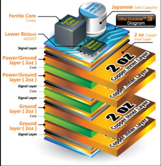
- Thermal Management: ECUs generate heat, especially in high-power applications like electric vehicle control. Stackups with thicker copper layers (e.g., 2 oz instead of 1 oz) or thermal vias can dissipate heat more effectively.
Key Considerations in ECU PCB Layer Stackup Design
Designing a layer stackup for an ECU PCB involves balancing multiple factors to meet performance and reliability goals. Let’s break down the most important considerations for automotive applications.
1. Number of Layers
The number of layers in an ECU PCB depends on the complexity of the circuit and the density of components. A basic ECU for a simple function like window control might use a 4-layer board, while a complex engine management system could require 8 or more layers. Here’s a typical breakdown:
- 4-Layer Stackup: Often used for simpler ECUs. A common arrangement is Signal-Power-Ground-Signal, where the internal power and ground planes shield the outer signal layers.
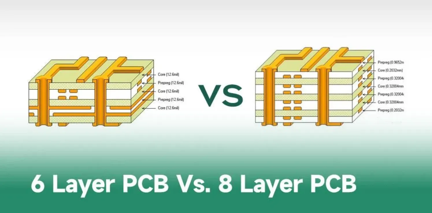
- 6-Layer Stackup: Suitable for mid-range ECUs with moderate signal density. A typical configuration might be Signal-Ground-Signal-Power-Ground-Signal, providing better EMI shielding and impedance control.
- 8+ Layer Stackup: Used for advanced ECUs with high-speed signals and multiple power domains. These stackups allow for dedicated layers for different signal types (e.g., analog vs. digital) and additional ground planes for noise isolation.
2. Layer Arrangement for Signal and Power Integrity
Signal and power integrity in ECU PCBs are non-negotiable for reliable operation. The arrangement of layers directly affects how signals and power are managed. Best practices include:
- Adjacent Ground Planes: Place ground planes next to signal layers to provide a low-impedance return path for high-speed signals. This reduces signal reflection and crosstalk.
- Power Plane Placement: Position power planes near ground planes to create a low-inductance path for decoupling capacitors, minimizing power supply noise.
- Signal Layer Separation: Route high-speed signals on outer layers or separate them from noisy power lines to avoid interference. For example, keep analog sensor signals on a different layer from digital communication lines.
For a 6-layer board, a recommended stackup for signal and power integrity might look like this: Top Signal, Ground, Inner Signal 1, Power, Ground, Bottom Signal. This setup ensures that every signal layer has an adjacent reference plane for controlled impedance.
3. Automotive PCB Impedance Control
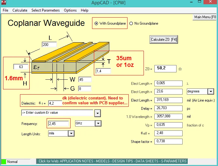
Impedance control is a cornerstone of high-speed ECU design. Mismatched impedance can cause signal reflections, leading to data errors in critical systems like ABS or engine control. To achieve precise impedance (e.g., 50 ohms for single-ended or 90 ohms for differential pairs), consider:
- Trace Width and Spacing: Use a PCB design tool to calculate trace dimensions based on the dielectric constant of the material and layer thickness. For a 1.6mm thick board with FR-4 material (dielectric constant ~4.4), a 50-ohm trace might be around 0.3mm wide on the top layer with a ground plane below.
- Dielectric Thickness: Thinner dielectric layers between signal and reference planes result in tighter impedance control but may increase manufacturing costs.
- Reference Planes: Ensure that signal traces are routed over continuous ground or power planes to maintain consistent impedance. Avoid splitting planes under high-speed traces.
Impedance control is especially critical for protocols like CAN FD or Ethernet used in modern vehicles, where data rates can exceed 5 Mbps. A mismatch as small as 10% can degrade signal quality, leading to communication failures.
4. PCB Material Selection for ECU Applications
Material selection for ECU PCBs is crucial due to the harsh operating conditions in automotive environments. The substrate and copper thickness must withstand temperature extremes, humidity, and mechanical stress. Common considerations include:
- FR-4: A standard material for many ECU PCBs due to its cost-effectiveness and good electrical properties. However, standard FR-4 may not suffice for high-temperature applications (above 105°C). High-Tg FR-4, with a glass transition temperature of 170°C or higher, is often preferred.
- Polyimide: Used in high-reliability ECUs due to its excellent thermal stability (up to 260°C) and flexibility, though it’s more expensive.
- Copper Thickness: Automotive PCBs often use 1 oz (35 μm) or 2 oz (70 μm) copper for better current-carrying capacity and heat dissipation, especially in power-heavy ECUs.
- Thermal Conductivity: Materials with higher thermal conductivity (e.g., metal-core PCBs for some power ECUs) help manage heat in high-current applications.
Choosing the right material ensures the PCB can endure the automotive environment while maintaining electrical performance. For instance, an ECU in an electric vehicle battery management system might use a high-Tg material to handle elevated temperatures near the battery pack.
Best Practices for Automotive PCB Stackup Design
To achieve optimal performance in ECU PCBs, follow these best practices during the design phase:
- Simulate Before Manufacturing: Use simulation tools to model signal integrity, power distribution, and thermal behavior of your stackup. This helps identify issues like impedance mismatches or hot spots before prototyping.
- Minimize Layer Transitions: Keep high-speed signals on a single layer whenever possible to avoid vias, which introduce inductance and can degrade signal quality.
- Use Symmetrical Stackups: Design symmetrical stackups (e.g., equal dielectric thicknesses on both sides of the board center) to prevent warpage during manufacturing and under thermal stress.
- Collaborate with Fabricators: Work closely with your PCB manufacturer to ensure the stackup design is manufacturable and cost-effective. Discuss dielectric materials, layer thicknesses, and copper weights early in the process.
- Adhere to Standards: Follow automotive industry standards like ISO 26262 for functional safety and IPC-6012 for PCB qualification to ensure reliability and compliance.
Challenges in ECU PCB Layer Stackup Design
Designing a stackup for automotive ECUs isn’t without challenges. Engineers often face trade-offs between performance, cost, and manufacturability. Some common hurdles include:
- Space Constraints: Modern vehicles pack more electronics into smaller spaces, forcing designers to use high-density stackups with thinner dielectrics, which can increase costs.
- High-Speed Requirements: As automotive systems adopt faster communication protocols (e.g., Automotive Ethernet at 100 Mbps or higher), maintaining signal integrity becomes more complex, requiring precise impedance control.
- Cost Pressures: Automotive manufacturers demand high reliability at low cost, which can limit material choices and layer counts.
- Environmental Stress: ECUs must operate reliably under extreme conditions, pushing the limits of standard materials and stackup designs.
Overcoming these challenges requires careful planning, advanced design tools, and collaboration with experienced PCB fabricators who understand automotive requirements.
Conclusion: Building Reliable ECU PCBs with Optimal Stackup Design
A well-designed layer stackup is the foundation of high-performance ECU PCBs in automotive applications. By focusing on the right number of layers, strategic layer arrangement, automotive PCB impedance control, and proper material selection, engineers can ensure signal and power integrity while meeting the rigorous demands of the automotive environment. Whether you’re working on a simple 4-layer board for a basic control unit or an advanced 8-layer design for a cutting-edge autonomous driving system, the principles of ECU PCB layer stackup design remain the same: prioritize performance, reliability, and manufacturability.
At ALLPCB, we’re committed to supporting your automotive PCB projects with high-quality manufacturing and expert guidance. From initial stackup design to final production, our team is ready to help you achieve optimal ECU performance. Start your next project with confidence, knowing that every layer of your PCB is built for success.


