ALLPCB


In the world of PCB design, power plane decoupling is a critical concept for ensuring stable performance and minimizing noise in electronic circuits. If you're searching for answers on power plane decoupling capacitors, capacitor placement, reducing ground bounce, or power supply noise, you're in the right place. This guide will break down everything you need to know about effective decoupling strategies to optimize your PCB designs. We'll cover the fundamentals, dive into specific techniques, and provide actionable tips to help you achieve reliable power delivery and signal integrity.
What Is Power Plane Decoupling and Why Does It Matter?
Power plane decoupling is a technique used in PCB design to stabilize the voltage supply to integrated circuits (ICs) and other components by minimizing noise and voltage fluctuations. When ICs switch states rapidly, they draw sudden bursts of current, which can cause voltage drops or spikes in the power supply. These disturbances, often referred to as power supply noise, can lead to signal integrity issues, electromagnetic interference (EMI), and even system failures.
Decoupling involves placing capacitors near ICs to act as local energy reservoirs. These capacitors supply the sudden current demands of the ICs, reducing the impact of noise and maintaining a steady voltage. Without proper decoupling, you risk issues like ground bounce—a phenomenon where the ground plane voltage fluctuates due to rapid current changes—potentially disrupting the operation of your circuit.
In this comprehensive guide, we'll explore the role of power plane decoupling capacitors, best practices for capacitor placement, and proven strategies for reducing ground bounce and power supply noise. Whether you're a seasoned engineer or just starting with PCB design, this resource will equip you with the knowledge to build more reliable and efficient circuits.
Understanding Power Plane Decoupling Capacitors
Power plane decoupling capacitors, often called bypass capacitors, are essential components in PCB design. Their primary function is to filter out high-frequency noise from the power supply and provide a stable voltage to ICs during rapid switching events. These capacitors act as a buffer, storing charge locally and releasing it when the IC demands a sudden surge of current.
There are typically two types of decoupling capacitors used in PCB designs:
- Bulk Capacitors: These are larger capacitors (often in the range of 10 μF to 100 μF) that handle low-frequency noise and provide a reservoir of charge for the entire board.
- Ceramic Capacitors: These are smaller (typically 0.01 μF to 1 μF) and handle high-frequency noise. They are placed closer to the ICs for immediate current delivery.
The effectiveness of decoupling capacitors depends on their value, type, and placement. For example, a 0.1 μF ceramic capacitor is often used for high-frequency noise suppression near an IC's power pin, while a 10 μF tantalum capacitor might be placed further away to address lower-frequency fluctuations.
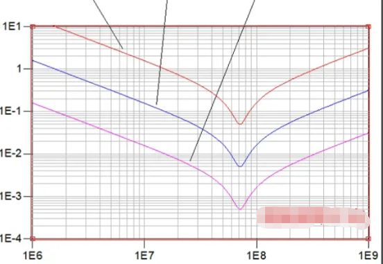
Without these capacitors, the impedance of the power delivery network (PDN) can increase at certain frequencies, leading to voltage drops. A well-designed decoupling strategy ensures that the PDN impedance remains below a target value—often less than 1 mΩ at critical frequencies—to maintain signal integrity.
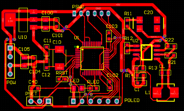
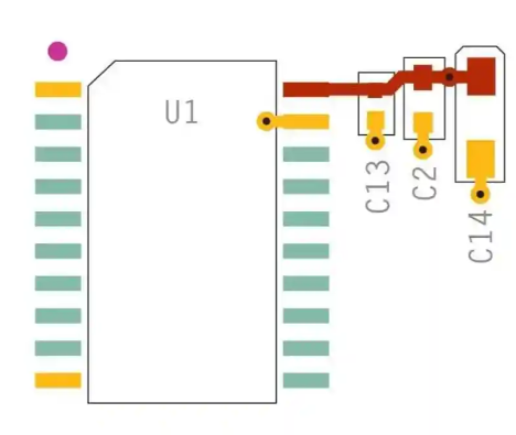
Capacitor Placement: Best Practices for Optimal Performance
Capacitor placement is just as important as selecting the right capacitor value. Poor placement can negate the benefits of decoupling, leaving your circuit vulnerable to noise and ground bounce. Here are some key guidelines for effective capacitor placement in your PCB layout:
1. Place Capacitors Close to IC Power Pins
The closer a decoupling capacitor is to the power pin of an IC, the more effective it will be. This minimizes the inductance of the traces connecting the capacitor to the IC, allowing for faster current delivery. Ideally, place capacitors within 1-2 mm of the power pin. For high-speed ICs, such as microcontrollers or FPGAs, this distance is even more critical.
2. Use Short, Wide Traces or Vias
Long, narrow traces introduce additional inductance, which can reduce the capacitor's ability to respond to rapid current changes. Use short, wide traces or connect the capacitor directly to the power and ground planes through vias. This keeps the loop inductance low—often below 1 nH for high-frequency applications.
3. Prioritize Multiple Capacitors for Different Frequencies
A single capacitor cannot effectively handle all noise frequencies. Use a combination of capacitors with different values (e.g., 0.01 μF, 0.1 μF, and 1 μF) near each IC to cover a broad frequency range. Place the smallest value capacitor closest to the power pin for high-frequency noise, followed by larger values for mid-range frequencies.
4. Distribute Capacitors Across the Board
For larger boards with multiple ICs, distribute bulk capacitors across the power plane to maintain a stable voltage throughout the PCB. This helps prevent voltage drops in areas far from the main power supply input.
Related Reading: Power Plane Segmentation and Decoupling Capacitor Placement
Strategies for Reducing Ground Bounce
Ground bounce is a common issue in high-speed digital circuits, where rapid switching of IC outputs causes the ground plane voltage to fluctuate. This can lead to false triggering of signals and degraded performance. Reducing ground bounce requires a combination of proper decoupling and thoughtful PCB design. Here are some proven techniques:
1. Minimize Loop Inductance with Proper Decoupling
Ground bounce is often caused by the inductance in the power and ground paths. By placing decoupling capacitors close to IC power pins and using low-inductance connections (short traces or vias), you can minimize the voltage fluctuations on the ground plane. Aim for a loop inductance of less than 0.5 nH for high-speed designs.
2. Use Continuous Ground Planes
A solid, continuous ground plane provides a low-impedance return path for currents, reducing the likelihood of ground bounce. Avoid splitting the ground plane unless absolutely necessary, as splits can create high-impedance paths and worsen noise issues.
3. Limit Simultaneous Switching Outputs (SSO)
Ground bounce is more pronounced when multiple outputs of an IC switch simultaneously. If possible, design your circuit to stagger switching events or use ICs with built-in slew rate control to reduce the rate of current change.
4. Add Local Ground Vias
For ICs with multiple ground pins, connect each pin to the ground plane with a dedicated via. This minimizes the inductance of the ground connection and helps distribute return currents evenly, reducing ground bounce.

Power Supply Noise Reduction Techniques
Power supply noise can degrade the performance of sensitive analog and digital circuits. Beyond proper decoupling capacitor placement, several additional strategies can help reduce power supply noise in your PCB design.
1. Optimize Power Plane Design
Design your power plane to have low impedance across a wide frequency range. Use wide power traces or dedicated power planes to minimize resistance and inductance. For multilayer boards, place power and ground planes adjacent to each other to create a natural capacitance (often around 1 nF per square inch) that aids in high-frequency noise suppression.
2. Use Ferrite Beads for Additional Filtering
Ferrite beads, in series with the power supply line, can filter out high-frequency noise before it reaches sensitive components. Combine a ferrite bead with a bulk capacitor to create a low-pass filter, effectively reducing noise above 1 MHz.
3. Isolate Sensitive Circuits
For mixed-signal designs, isolate analog and digital sections of the board to prevent digital switching noise from affecting analog circuits. Use separate power planes or split planes with a single-point connection to maintain a clean reference ground for analog components.
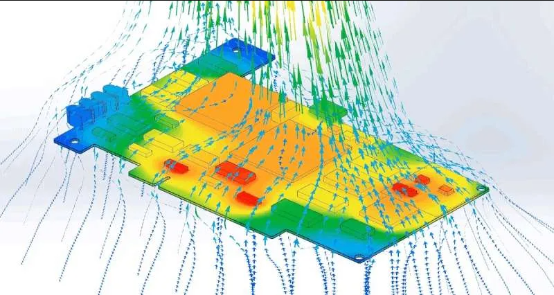
4. Monitor PDN Impedance
Use simulation tools to analyze the impedance of your power delivery network across different frequencies. Target an impedance below 1 mΩ at frequencies where your ICs operate to ensure minimal voltage ripple. Adjust capacitor values and placement based on simulation results for optimal performance.
Related Reading: Decoding Capacitor Codes: A Comprehensive Guide for Engineers
Effective Decoupling Strategies for PCB Design
Now that we've covered the basics of power plane decoupling capacitors, placement, and noise reduction techniques, let's tie it all together with actionable decoupling strategies for your PCB designs. These strategies will help you achieve reliable power delivery and signal integrity, even in complex, high-speed applications.
1. Layer Stackup Planning
Plan your PCB layer stackup to minimize noise. Place power and ground planes on adjacent layers to maximize interplane capacitance, which helps with high-frequency decoupling. For a 4-layer board, a common stackup is signal-power-ground-signal, ensuring tight coupling between power and ground.
2. Use a Range of Capacitor Values
As mentioned earlier, a single capacitor value cannot address all noise frequencies. Use a combination of capacitor values—such as 0.01 μF, 0.1 μF, and 10 μF—to cover a frequency range from 100 kHz to 100 MHz. This ensures comprehensive noise suppression across the spectrum.
3. Simulate and Test Your Design
Before finalizing your PCB layout, simulate the power delivery network to identify potential issues with impedance or resonance. Tools like SPICE or dedicated PDN analysis software can help you fine-tune capacitor placement and values. After fabrication, test your board with an oscilloscope to measure voltage ripple and confirm that noise levels are within acceptable limits (e.g., less than 50 mV peak-to-peak for most digital ICs).
4. Follow Manufacturer Guidelines
Many IC manufacturers provide specific decoupling recommendations in their datasheets. These guidelines often include suggested capacitor values, placement distances, and even layout diagrams. Always review these documents to ensure compliance with the IC's requirements for stable operation.
Common Mistakes to Avoid in Power Plane Decoupling
Even with the best intentions, it's easy to make mistakes in power plane decoupling that can compromise your design. Here are some common pitfalls to watch out for:
- Placing Capacitors Too Far from ICs: Distance increases inductance, reducing the capacitor's effectiveness. Always prioritize proximity over convenience in layout.
- Using Insufficient Capacitor Values: A single capacitor or incorrect value won't cover the full frequency range of noise. Use multiple values for comprehensive protection.
- Ignoring Ground Plane Integrity: Cuts or splits in the ground plane can create high-impedance paths, worsening ground bounce and noise.
- Overlooking Simulation: Skipping PDN simulation can lead to unexpected resonance or impedance issues that only become apparent after fabrication.
Conclusion: Mastering Power Plane Decoupling for Better PCB Performance
Power plane decoupling is a cornerstone of reliable PCB design. By understanding the role of decoupling capacitors, mastering capacitor placement, and implementing strategies for reducing ground bounce and power supply noise, you can significantly improve the performance and stability of your circuits. Whether you're working on a simple microcontroller project or a complex high-speed system, these principles will help you achieve optimal power delivery and signal integrity.
Start by selecting the right combination of capacitors for your design, place them strategically near IC power pins, and use a solid ground plane to minimize noise. Leverage simulation tools to fine-tune your power delivery network, and always adhere to manufacturer recommendations for the best results. With these decoupling strategies in hand, you're well-equipped to tackle even the most demanding PCB designs with confidence.