 ALLPCB


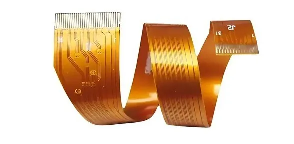
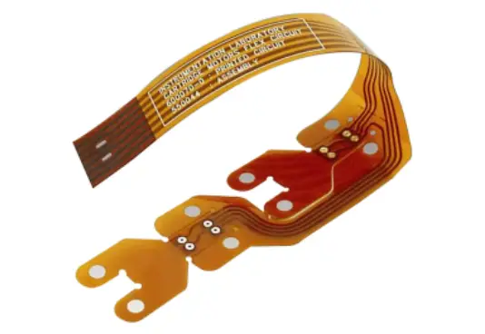
Are you designing a flexible PCB and wondering about the right copper thickness for your project? Copper thickness, measured in microns, plays a critical role in the performance, flexibility, and durability of flexible PCBs. Whether you're working on wearable electronics or complex flex circuits, understanding copper thickness is key to achieving optimal results. In this comprehensive guide, we'll dive deep into copper thickness in flexible PCB design, its impact on bend radius, material choices, and applications like wearable electronics. Let's explore how to make informed decisions for your next project with practical insights and actionable tips.
Why Copper Thickness Matters in Flexible PCB Design
Copper thickness is one of the most important factors in flexible PCB design. It directly affects the board's ability to conduct electricity, handle current, and withstand bending without cracking or breaking. In flexible PCBs, copper is typically measured in microns (μm) or ounces per square foot (oz/ft2), where 1 oz/ft2 equals approximately 35 microns. Choosing the right thickness ensures a balance between flexibility, durability, and electrical performance.
For applications like wearable electronics, where space and weight are limited, thinner copper layers are often preferred. However, for high-current applications, thicker copper may be necessary to prevent overheating and ensure reliability. Striking the right balance is crucial, and this guide will help you understand the factors that influence your choice.
Understanding Copper Thickness in Flexible PCBs
Copper thickness in flexible PCBs typically ranges from 9 microns (0.25 oz/ft2) to 70 microns (2 oz/ft2), depending on the application. Here's a breakdown of common thicknesses and their uses:
- 9-12 microns (0.25-0.33 oz/ft2): Ultra-thin copper, ideal for highly flexible designs and wearable electronics where minimal weight and maximum bendability are required.
- 18 microns (0.5 oz/ft2): A common choice for many flex PCB designs, offering a good balance between flexibility and current-carrying capacity.
- 35 microns (1 oz/ft2): Standard thickness for applications needing moderate current handling, often used in dynamic flex circuits.
- 70 microns (2 oz/ft2): Thicker copper for high-current applications, though less common in flexible PCBs due to reduced flexibility.
The thinner the copper, the more flexible the PCB becomes, but this comes at the cost of reduced current capacity and durability. On the other hand, thicker copper improves conductivity and strength but limits how much the board can bend without damage.
How Copper Thickness Affects Bend Radius in Flex PCBs
The bend radius is the minimum radius a flexible PCB can be bent without causing damage to the copper traces or the substrate. Copper thickness has a direct impact on this parameter. Thinner copper allows for a tighter bend radius, making it ideal for applications requiring frequent or sharp bending, such as foldable devices or wearable electronics.
As a general rule, the bend radius should be at least 6-10 times the total thickness of the flexible PCB (including copper and substrate layers) for dynamic bending applications. For static bending (where the board is bent once and remains in position), a bend radius of 3-6 times the thickness may suffice. For example, a flex PCB with a total thickness of 100 microns (including a 12-micron copper layer) should have a minimum bend radius of 600-1000 microns for dynamic use.
Using thicker copper increases the overall thickness and stiffness of the board, requiring a larger bend radius to prevent cracking. If your design involves tight bends, opting for a copper thickness of 9-18 microns can help maintain flexibility while still providing adequate conductivity.
Choosing the Right Copper Thickness for Your Application
Selecting the appropriate copper thickness for your flexible PCB depends on several factors, including current requirements, flexibility needs, and environmental conditions. Let's explore how to make the right choice for different scenarios.
1. Current-Carrying Capacity
The amount of current your PCB needs to handle is a primary consideration. Thicker copper can carry more current without overheating. For instance, a trace with 18-micron copper might safely handle up to 1-2 amps, depending on trace width and ambient temperature, while a 35-micron copper trace can handle 3-5 amps under similar conditions. If you're designing a power circuit for a wearable device, calculate the expected current load and choose a thickness that supports it without excessive heat buildup.
2. Flexibility and Bend Requirements
For applications requiring frequent bending, such as in foldable displays or medical wearables, thinner copper (9-18 microns) is often the best choice. Thicker copper (35-70 microns) may be more suitable for static flex applications where the board is bent once during assembly and remains fixed.
3. Environmental Factors
Environmental conditions like temperature and humidity can affect the performance of copper in flexible PCBs. Thinner copper is more susceptible to cracking under thermal stress, so consider using a slightly thicker layer (e.g., 18 microns instead of 9 microns) if the device will operate in harsh conditions.
4. Cost Considerations
Thicker copper layers generally cost more due to increased material usage and manufacturing complexity. If budget is a concern, balance the need for performance with cost by selecting the thinnest copper layer that meets your electrical and mechanical requirements.
Flex PCB Materials and Their Role in Copper Thickness Selection
The substrate and adhesive materials used in flexible PCBs also influence the choice of copper thickness. Common materials include:
- Polyimide (PI): The most widely used substrate for flex PCBs due to its excellent thermal stability and flexibility. Polyimide works well with copper thicknesses ranging from 9 to 35 microns, making it versatile for various applications.
- Polyester (PET): A cost-effective option for less demanding applications. PET is typically paired with thinner copper (9-18 microns) due to its lower thermal resistance.
- Adhesiveless Laminates: These materials bond copper directly to the substrate without adhesives, reducing overall thickness and improving flexibility. They are ideal for ultra-thin copper layers in wearable electronics.
The material's properties, such as tensile strength and thermal expansion, must align with the copper thickness to prevent delamination or cracking during bending. For example, using a 70-micron copper layer on a thin polyimide substrate might cause stress concentration and failure during bending, so pairing thicker copper with a more robust substrate is often necessary.
Copper Thickness in Wearable Electronics: A Special Case
Wearable electronics, such as smartwatches, fitness trackers, and medical sensors, demand unique considerations for flexible PCB design. These devices require lightweight, compact, and highly flexible circuits that conform to the body's shape. Copper thickness in these applications is often kept to a minimum—typically 9-12 microns—to achieve the necessary flexibility and reduce weight.
However, even in wearables, some components may require higher current, such as power delivery lines for batteries or LEDs. In such cases, a hybrid approach can be used, where critical traces are designed with slightly thicker copper (18 microns) while maintaining thinner copper for the rest of the circuit. This ensures both flexibility and performance without compromising the design.
Additionally, wearable electronics often operate in dynamic environments, requiring frequent bending. A tight bend radius is essential, and thinner copper helps achieve this. For instance, a wearable sensor with a total PCB thickness of 80 microns might achieve a bend radius as low as 480-800 microns, allowing it to wrap comfortably around a wrist or other body part.
Design Tips for Optimizing Copper Thickness in Flexible PCBs
Designing a flexible PCB with the right copper thickness involves more than just picking a number. Here are some practical tips to ensure success:
- Use Simulation Tools: Leverage design software to simulate bending and current flow. This can help predict how different copper thicknesses will perform under real-world conditions.
- Minimize Copper in Bend Areas: If possible, avoid placing thick copper traces in areas that will experience frequent bending. Instead, route critical traces away from high-stress zones.
- Consider Multilayer Designs: For complex circuits, use multilayer flex PCBs with varying copper thicknesses. Thinner copper can be used for signal layers, while thicker copper supports power delivery.
- Test Prototypes: Before mass production, create prototypes with different copper thicknesses to test flexibility, durability, and electrical performance under actual operating conditions.
- Consult with Manufacturers: Work closely with your PCB fabricator to understand their capabilities and limitations regarding copper thickness and material compatibility.
Common Challenges with Copper Thickness in Flex PCB Design
While copper thickness is a critical design parameter, it can also present challenges if not addressed properly. Here are some common issues and how to mitigate them:
- Cracking of Copper Traces: Thicker copper is more prone to cracking during bending. Use thinner copper in dynamic areas and ensure the bend radius is within recommended limits.
- Overheating: Thin copper may overheat under high current loads. Increase trace width or use a slightly thicker copper layer for power traces to manage heat dissipation.
- Manufacturing Constraints: Not all fabricators can handle ultra-thin or very thick copper layers in flexible PCBs. Verify manufacturing capabilities early in the design process.
Conclusion: Making Informed Decisions on Copper Thickness
Choosing the right copper thickness for your flexible PCB is a balancing act between electrical performance, mechanical flexibility, and cost. Whether you're designing for wearable electronics or other innovative applications, understanding the impact of copper thickness on bend radius, material compatibility, and current capacity is essential. By considering the specific needs of your project and following best practices, you can create reliable and efficient flex PCB designs that meet your goals.
From ultra-thin 9-micron copper for maximum flexibility to thicker 35-micron layers for higher current handling, each option has its place in flexible PCB design. Take the time to evaluate your requirements, test different configurations, and collaborate with experienced manufacturers to achieve the best results. With the insights provided in this guide, you're well-equipped to tackle the challenges of copper thickness and create cutting-edge flexible circuits.


