 ALLPCB


In the fast-evolving world of electronics, High-Density Interconnect (HDI) PCBs are at the forefront of enabling smaller, faster, and more efficient devices. One key feature that makes HDI technology stand out is the use of blind vias. But what exactly are the HDI PCB blind via advantages, and why should engineers consider them for their designs? In short, blind vias offer improved signal integrity, reduced board size, enhanced reliability, and potential cost savings when planned correctly. This blog dives deep into these benefits, exploring aspects like blind via cost vs performance, blind via signal integrity benefits, and their role in high-speed PCB blind vias applications. Let’s uncover the hidden potential of blind vias and see how they can elevate your next project.
What Are Blind Vias in HDI PCBs?
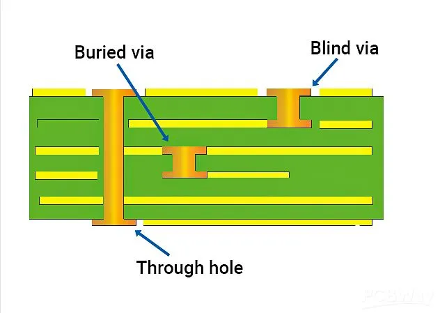
Before we explore the advantages, let’s define what blind vias are. A blind via is a type of vertical interconnect access (via) in a printed circuit board (PCB) that connects an outer layer to an inner layer but does not go through the entire board. Unlike traditional through-hole vias that span all layers, blind vias are only visible from one side of the board, typically created using laser drilling for precision and plated with copper for conductivity.
In HDI PCBs, where space is limited and component density is high, blind vias play a critical role. They allow designers to connect specific layers without occupying unnecessary space on other layers, freeing up room for additional routing and components. This targeted connectivity is what makes blind vias a game-changer in modern PCB design, especially for compact and high-performance applications like smartphones, wearables, and medical devices.
Key Advantages of Blind Vias in HDI PCB Design
Blind vias bring several unique benefits to the table, making them a preferred choice for engineers working on high-density and high-speed designs. Below, we break down the most significant HDI PCB blind via advantages with detailed explanations and practical insights.
1. Space Optimization for Compact Designs
One of the standout benefits of blind vias is their ability to save space. In traditional PCB designs with through-hole vias, every via takes up space across all layers, even if it’s only needed to connect two specific layers. Blind vias, on the other hand, stop at the required inner layer, leaving the remaining layers free for other traces or components. This is especially crucial in HDI PCBs, where every square millimeter counts.
For example, in a six-layer board, a blind via might connect layer 1 to layer 2 without affecting layers 3 through 6. This can reduce the overall board size by up to 20-30% in some designs, allowing for more compact products without sacrificing functionality. Smaller boards also mean less material usage, which can lower production costs in high-volume manufacturing.
2. Enhanced Signal Integrity for High-Speed Applications
When it comes to blind via signal integrity benefits, the impact is significant, especially in high-speed PCB blind vias applications. Signal integrity refers to the quality of an electrical signal as it travels through the PCB. Poor signal integrity can lead to data loss, noise, or delays, which are unacceptable in high-speed designs like 5G devices or high-frequency communication systems.
Blind vias improve signal integrity by shortening signal paths. Since they don’t pass through unnecessary layers, they reduce the length of the conductive path, minimizing signal reflection and crosstalk. Additionally, blind vias eliminate "stubs"—unused portions of a via that can act as antennas and cause signal distortion. For instance, in a design operating at 10 GHz, removing stubs with blind vias can reduce signal loss by as much as 0.5 dB per inch of trace length, ensuring cleaner and faster data transmission.
3. Increased Routing Density and Flexibility
HDI PCBs often require intricate routing to accommodate numerous components in a small area. Blind vias provide greater routing flexibility by freeing up space on layers not involved in the connection. This allows designers to place more traces and components on each layer, achieving higher circuit density without increasing the board’s footprint.
For instance, in a multilayer HDI PCB used in a wearable device, blind vias can enable a 50% increase in trace density on inner layers compared to a design relying solely on through-hole vias. This added flexibility is invaluable for modern electronics, where miniaturization is a constant goal.
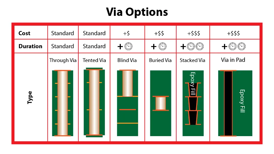
4. Improved Reliability with Smaller Aspect Ratios
Reliability is a critical factor in any PCB design, and blind vias offer an edge here as well. Due to their smaller depth compared to through-hole vias, blind vias typically have a lower aspect ratio (the ratio of via depth to diameter). A lower aspect ratio, often around 1:1 or less in HDI designs, makes them easier to plate with copper during manufacturing, reducing the risk of defects like voids or incomplete plating.
This reliability is particularly important in applications exposed to harsh conditions, such as automotive electronics or aerospace systems. A well-manufactured blind via can withstand thermal cycling and mechanical stress better than a deeper through-hole via, ensuring long-term performance.
Blind Via Cost vs Performance: Striking the Right Balance
A common concern among engineers is the blind via cost vs performance trade-off. At first glance, blind vias might seem more expensive due to the advanced manufacturing techniques required, such as laser drilling and precise layer alignment. However, when planned strategically, they can lead to overall cost savings while boosting performance.
Manufacturing Costs of Blind Vias
The cost of incorporating blind vias largely depends on the complexity of the design and the manufacturing process. Laser drilling, used for creating small-diameter blind vias (often less than 150 micrometers), is more expensive than mechanical drilling used for through-hole vias. Additionally, HDI boards with blind vias may require sequential lamination, where layers are built up step by step, adding to the production time and cost.
On average, the cost of an HDI PCB with blind vias can be 10-20% higher per square inch compared to a standard PCB with through-hole vias. However, this cost is often offset by the reduced board size and fewer layers needed in the design. For high-volume production, the savings from material reduction can outweigh the initial manufacturing expense.
Performance Gains Justify the Investment
From a performance standpoint, the investment in blind vias is often worth it. The signal integrity improvements alone can make a significant difference in high-speed applications, where even a small reduction in noise or delay can impact the end product’s functionality. For example, in a 5G communication module, using blind vias to optimize signal paths can improve data rates by up to 15%, directly translating to better user experience and product competitiveness.
Moreover, the space savings from blind vias can reduce the number of layers required in a PCB stack-up. A design that might need eight layers with through-hole vias could be achieved in six layers with blind vias, cutting material and fabrication costs by a noticeable margin.
Applications of Blind Vias in High-Speed PCB Designs
Blind vias are particularly valuable in high-speed PCB blind vias applications, where performance and space constraints are critical. Here are a few areas where they shine:
- Telecommunications: In 5G infrastructure and devices, blind vias help manage high-frequency signals (up to 28 GHz and beyond) by minimizing signal loss and crosstalk.
- Consumer Electronics: Smartphones and tablets rely on HDI PCBs with blind vias to pack powerful processors, memory, and sensors into ultra-thin form factors.
- Medical Devices: Compact diagnostic tools and wearable health monitors use blind vias to achieve high functionality in small, portable designs.
- Automotive Systems: Advanced driver-assistance systems (ADAS) and infotainment units benefit from the reliability and signal integrity of blind vias under varying environmental conditions.
Design Considerations for Implementing Blind Vias
While blind vias offer numerous advantages, their implementation requires careful planning to maximize benefits and avoid potential pitfalls. Here are some key considerations for engineers:
Stack-Up Planning
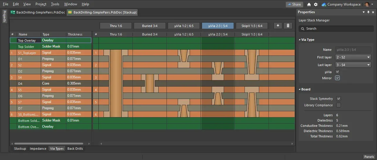
Designing an HDI PCB with blind vias starts with a well-thought-out layer stack-up. Determine which layers need to be connected via blind vias and ensure that the manufacturing process supports the required via depths and diameters. A typical HDI stack-up might include blind vias between layers 1-2 and 5-6, with buried vias for inner-layer connections, optimizing both space and cost.
Via Size and Aspect Ratio
Blind vias in HDI designs often use microvias with diameters as small as 100-150 micrometers. Keeping the aspect ratio low (ideally 0.75:1 to 1:1) ensures reliable plating and minimizes manufacturing defects. Work closely with your fabrication partner to confirm their capabilities for microvia drilling and plating.
Signal Integrity Analysis
Use simulation tools to analyze signal integrity before finalizing the design. Pay attention to impedance matching, especially in high-speed applications. For example, maintaining a 50-ohm impedance for high-frequency signals might require adjusting trace widths and via placements to avoid discontinuities caused by blind vias.
Challenges and Limitations of Blind Vias
Despite their many benefits, blind vias are not without challenges. Manufacturing complexity is a primary concern, as laser drilling and sequential lamination require advanced equipment and skilled technicians. This can lead to longer lead times and higher costs for prototypes or low-volume runs.
Additionally, blind vias are not suitable for all applications. In designs where thermal dissipation is a priority, through-hole vias might be preferred due to their ability to conduct heat across all layers. Engineers must weigh these factors based on the specific needs of their project.
How to Get Started with Blind Vias in Your HDI PCB Design
If you’re considering blind vias for your next HDI PCB project, start by partnering with a reliable fabrication service that has experience with HDI technology. Provide detailed design files and specifications, including via types, layer connections, and impedance requirements. Collaboration during the early design phase can help identify potential issues and optimize the layout for both performance and cost.
Additionally, invest in design software that supports HDI features and signal integrity simulations. This will allow you to test different configurations of blind vias and ensure they meet your project’s requirements before moving to production.
Conclusion: Unlock the Potential of Blind Vias in HDI PCBs
Blind vias are a powerful tool in the world of High-Density Interconnect PCBs, offering hidden advantages that can transform your design. From space optimization and enhanced blind via signal integrity benefits to improved reliability and routing flexibility, their impact is undeniable in modern electronics. While the blind via cost vs performance balance requires careful consideration, the long-term gains in efficiency and functionality often justify the investment, especially for high-speed PCB blind vias applications.
By understanding and leveraging the HDI PCB blind via advantages, engineers can push the boundaries of what’s possible in compact, high-performance designs. Whether you’re working on cutting-edge telecommunications equipment or a next-generation consumer gadget, blind vias could be the key to achieving your goals. Start exploring their potential today and see how they can elevate your PCB projects to new heights.


