Curious about how CT scanners and PCB technology have transformed medical imaging over the years? This blog post dives into the history of CT scanners, the role of PCB technology in their development, and how components, designs, and manufacturing have evolved. We'll also explore current trends and future predictions for this critical technology in healthcare. Whether you're an engineer, a medical professional, or simply interested in tech history, this detailed guide will walk you through every step of this fascinating journey.
Introduction: The Birth of CT Scanners and PCB Technology
Computed Tomography (CT) scanners revolutionized medical imaging when they were first introduced in the early 1970s. These machines allowed doctors to see detailed cross-sectional images of the human body, a feat previously unimaginable. At the heart of this innovation lies Printed Circuit Board (PCB) technology, which has played a crucial role in making CT scanners more efficient, compact, and powerful over the decades. In this post, we’ll trace the history of CT scanners, explore how PCB technology has evolved alongside them, and look at the design trends, manufacturing advancements, and future predictions shaping this field.
The History of CT Scanners: A Groundbreaking Innovation
The story of CT scanners begins in 1971, when the first clinical CT scan was performed on a patient in the UK at Atkinson Morley Hospital. Developed by British engineer Godfrey Hounsfield, this early machine took hours to produce a single image with a resolution that, by today’s standards, would seem incredibly low. However, it marked the start of a new era in diagnostics, earning Hounsfield a Nobel Prize in 1979.
Early CT scanners were bulky, slow, and limited in their capabilities. They relied on basic electronic components and rudimentary circuit designs to process data. Over the decades, these machines have undergone significant changes, driven by advancements in computing power and, importantly, PCB technology. From single-slice scanners in the 1970s to modern multi-detector systems capable of capturing hundreds of images in seconds, the evolution of CT scanners is a testament to engineering innovation.
Key Milestones in CT Scanner Development
- 1971: First clinical CT scan performed, taking hours for a single image.
- 1980s: Introduction of spiral CT scanners, allowing continuous scanning and faster image acquisition.
- 1990s: Multi-slice CT scanners emerge, capturing multiple image slices simultaneously.
- 2000s: Advanced detectors and software improve image quality and reduce radiation exposure.
- 2020s: Integration of AI and ultra-fast scanning technologies for real-time diagnostics.
The Role of PCB Technology in Medical Imaging
PCBs are the backbone of modern electronics, and their evolution has directly influenced the capabilities of CT scanners. In the early days, PCBs in medical imaging devices were simple, single-layer boards with limited functionality. They were used primarily for basic signal processing and power distribution. As the demand for faster, more accurate imaging grew, so did the complexity of PCBs.
Today, PCBs in CT scanners are multi-layered, high-density interconnect (HDI) designs that handle high-speed data transmission, precise signal control, and power management. These boards integrate advanced components like microprocessors, sensors, and analog-to-digital converters, enabling real-time image processing and reducing scan times from hours to mere seconds.
Component Evolution in CT Scanner PCBs
The components on PCBs for CT scanners have seen dramatic improvements over the years. Here are some key changes:
- 1970s: Basic resistors, capacitors, and transistors on single-layer PCBs. Signal processing was slow, with data transfer rates in the range of kilobits per second.
- 1980s-1990s: Introduction of integrated circuits (ICs) and early microprocessors, allowing data rates to reach megabits per second.
- 2000s: Use of Field-Programmable Gate Arrays (FPGAs) and Application-Specific Integrated Circuits (ASICs) for faster processing, with signal speeds exceeding hundreds of megabits per second.
- 2020s: Advanced sensors and AI chips on HDI PCBs, supporting data rates in gigabits per second for real-time imaging.
These advancements in component technology have not only improved performance but also reduced the size and power consumption of CT scanners, making them more accessible for hospitals and clinics.
Design Trends in PCB Technology for CT Scanners
As CT scanners became more sophisticated, PCB design trends adapted to meet new challenges. Here are some notable trends that have shaped PCB technology in medical imaging:
Miniaturization and High-Density Interconnect (HDI)
Modern CT scanners require compact designs to fit into smaller spaces while maintaining high performance. HDI PCBs, with their fine traces and microvias, allow for greater component density. This means more functionality in a smaller footprint, critical for portable or vehicle-mounted CT equipment.
Improved Signal Integrity
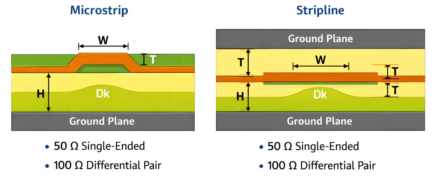
With high-speed data transfer becoming essential, PCB designs now focus on minimizing signal loss and interference. Techniques like controlled impedance (typically in the range of 50-100 ohms for high-speed lines) and differential pair routing ensure that data from detectors reaches processors without distortion.
Thermal Management
CT scanners generate significant heat due to high-power components. Modern PCB designs incorporate thermal vias, heat sinks, and advanced materials like ceramic substrates to dissipate heat efficiently, preventing damage to sensitive electronics.
Flexibility and Durability
Flexible and rigid-flex PCBs are increasingly used in CT scanners for areas requiring movement, such as rotating gantries. These boards withstand mechanical stress while maintaining reliable connections, a critical factor in high-use medical environments.
Manufacturing Advancements in PCB Technology for Medical Imaging
The manufacturing of PCBs for CT scanners has seen remarkable progress, driven by the need for precision, reliability, and scalability. Here’s how manufacturing techniques have evolved:
Automation and Precision
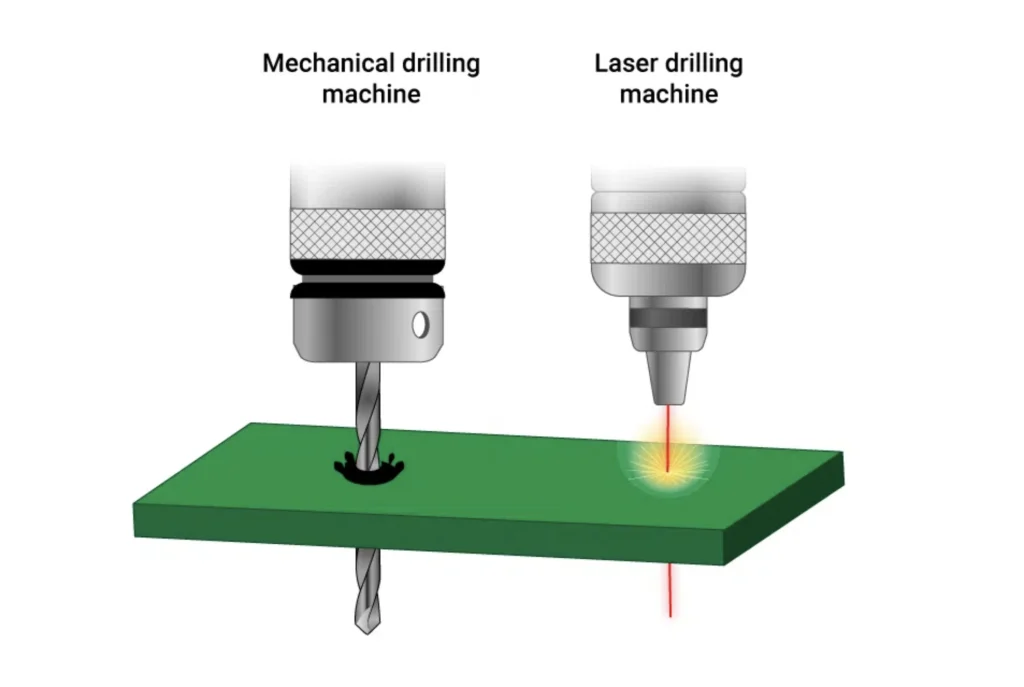
In the past, PCB manufacturing relied heavily on manual processes, leading to inconsistencies. Today, automated assembly lines use robotic systems for component placement with accuracy down to 0.01 mm, ensuring flawless integration in CT scanner electronics.
Advanced Materials
Early PCBs used basic FR-4 materials, which struggled with high-frequency signals and heat. Modern manufacturing employs high-performance materials like Rogers laminates and polyimide, which support signal integrity at frequencies above 1 GHz and withstand harsh operating conditions.
Quality Assurance
Medical imaging demands the highest reliability, as failures can impact patient safety. Advanced testing methods, such as Automated Optical Inspection (AOI) and X-ray inspection, detect defects in solder joints and internal layers, ensuring that every PCB meets strict standards.
Sustainable Practices
Recent years have seen a push toward eco-friendly manufacturing. Lead-free soldering and recyclable materials are now common, reducing the environmental impact of PCB production for medical devices.
Future Predictions for CT Scanner PCB Technology
The future of CT scanner PCB technology is exciting, with several trends poised to redefine medical imaging. Here are some predictions based on current developments:
Integration of Artificial Intelligence (AI)
AI is already being integrated into CT scanners for image reconstruction and diagnostics. Future PCBs will likely include dedicated AI processors, enabling on-device machine learning with data processing speeds exceeding 10 gigabits per second, reducing reliance on external systems.
Ultra-Compact Designs
As portable and mobile imaging solutions gain popularity, PCBs will become even smaller and more efficient. Innovations like 3D stacking and chip-on-board (COB) technology will pack more power into tiny spaces, ideal for vehicle-mounted CT equipment.
Enhanced Radiation Resistance
CT scanners expose electronics to radiation, which can degrade components over time. Future PCBs may use radiation-hardened materials and designs, extending the lifespan of scanners and reducing maintenance costs.
Wireless Connectivity
Emerging wireless technologies could eliminate the need for complex wiring in CT scanners. PCBs with built-in wireless modules will enable seamless data transfer between components, simplifying designs and improving reliability.
Conclusion: The Ongoing Journey of CT Scanner PCB Technology
The history of CT scanners and PCB technology is a story of relentless innovation. From the slow, bulky machines of the 1970s to today’s lightning-fast, AI-powered systems, every advancement has been supported by improvements in PCB design and manufacturing. As we look to the future, trends like AI integration, ultra-compact designs, and sustainable practices promise to push the boundaries of medical imaging even further.
At ALLPCB, we’re proud to be part of this journey, providing cutting-edge PCB solutions for the medical industry. Whether you’re designing the next generation of CT scanners or exploring other medical technologies, our expertise in high-quality, reliable PCB manufacturing can help bring your vision to life. Stay tuned to this space for more insights into the ever-evolving world of technology and healthcare.
 ALLPCB


