 ALLPCB


In the fast-evolving world of electronics, creating compact and efficient printed circuit boards (PCBs) is more important than ever. If you’re wondering how to fit more functionality into a smaller space, the answer lies in dense PCB design techniques, particularly through the use of embedded passives. By integrating components like resistors and capacitors directly into the PCB substrate, you can save valuable surface space, reduce parasitic effects, and improve performance. In this blog, we’ll dive deep into space-saving PCB techniques, focusing on embedded passives, component miniaturization, and High-Density Interconnect (HDI) PCB design strategies to help you master dense PCB layouts.
Why Dense PCB Design Matters in Modern Electronics
As devices like smartphones, wearables, and IoT gadgets shrink in size, engineers face the challenge of packing more power and functionality into limited space. Dense PCB design addresses this by maximizing the use of available board area. Traditional designs with surface-mounted components often lead to cluttered layouts, longer signal paths, and increased noise. By adopting advanced techniques like embedded passives and HDI PCB design, you can overcome these hurdles, achieving smaller footprints without sacrificing performance.
The benefits of dense PCB design are clear: reduced board size, lighter products, improved signal integrity, and lower manufacturing costs in high-volume production. Whether you’re working on a cutting-edge medical device or a compact consumer gadget, mastering space-saving PCB techniques is essential.
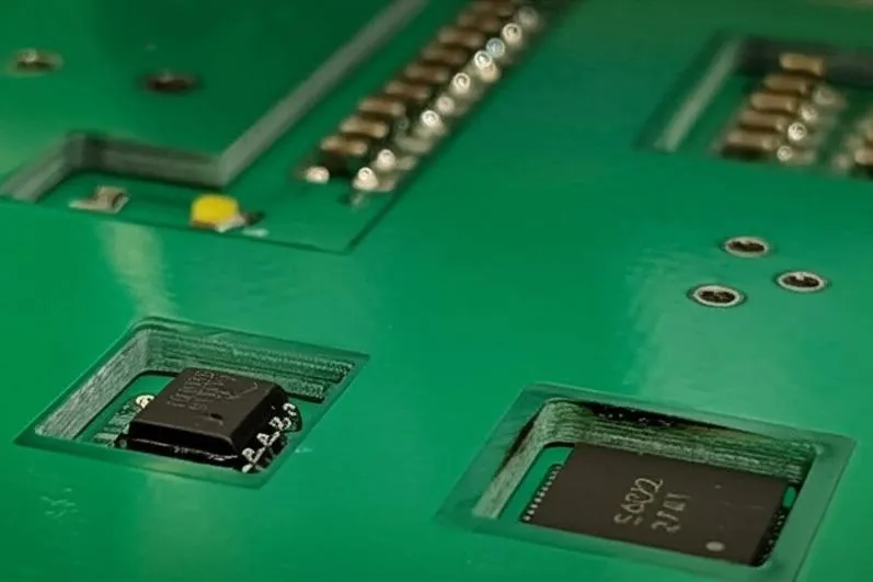
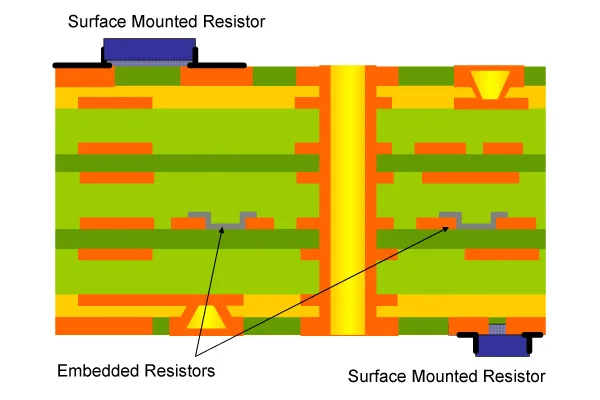
What Are Embedded Passives and How Do They Save Space?
Embedded passives are passive components, such as resistors, capacitors, and inductors, integrated directly into the layers of a PCB substrate rather than being mounted on the surface. This technique frees up valuable real estate on the board’s surface, allowing for a more compact layout and enabling the placement of additional active components.
Here’s how embedded passives contribute to space-saving PCB techniques:
- Reduced Surface Area: By moving passives inside the board, you eliminate the need for surface space typically occupied by discrete components.
- Shorter Signal Paths: Embedding components closer to active devices reduces trace lengths, minimizing signal delays and parasitic inductance. For example, a typical surface-mounted capacitor might introduce a parasitic inductance of 1-2 nH, while an embedded capacitor can reduce this to under 0.5 nH.
- Improved Reliability: With fewer soldered connections, the risk of mechanical failure due to vibration or thermal stress decreases.
Embedded passives are especially useful in high-frequency applications where signal integrity is critical. They help maintain stable impedance and reduce electromagnetic interference (EMI), making them ideal for RF and 5G designs.
Key Benefits of Embedded Passives in Dense PCB Design
Integrating passives into the PCB substrate offers several advantages beyond just saving space. Let’s explore these benefits in detail:
- Enhanced Miniaturization: With embedded passives, you can achieve component miniaturization by eliminating bulky discrete components. This is critical for applications like wearable technology, where every millimeter counts.
- Cost Efficiency in High Volumes: While the initial design and fabrication of PCBs with embedded passives can be complex, the reduced component count and simplified assembly process lower costs in large-scale production.
- Better Thermal Management: Embedded components are less exposed to external heat sources and can dissipate heat more effectively through the PCB substrate, improving overall thermal performance.
- Reduced Parasitic Effects: By placing passives closer to where they’re needed, you minimize unwanted capacitance and inductance, which can degrade performance at high frequencies (e.g., above 1 GHz).
These benefits make embedded passives a game-changer for engineers working on dense PCB design projects.
Space-Saving PCB Techniques: Beyond Embedded Passives
While embedded passives are a powerful tool, they’re just one part of the space-saving puzzle. Here are additional techniques to consider when designing dense PCBs:
1. Component Miniaturization
Choosing smaller components is a straightforward way to save space. Modern passive components, such as 0201 or even 01005 size resistors and capacitors, are incredibly tiny, allowing you to fit more onto the board. However, working with such small components requires precise placement and soldering equipment, as well as careful attention to thermal and electrical constraints.
2. Multi-Layer PCB Design
Using multiple layers in your PCB allows you to stack components and traces vertically rather than spreading them out horizontally. A 6-layer or 8-layer board can house complex circuits in a fraction of the surface area compared to a single- or double-layer design. This approach is often paired with embedded passives for maximum density.
3. High-Density Interconnect (HDI) PCB Design
HDI PCB design is a cornerstone of dense layouts. It involves using microvias, blind vias, and buried vias to connect layers with finer traces and smaller pads. HDI techniques enable higher component density and shorter interconnects, reducing signal loss and improving performance. For instance, HDI designs can achieve trace widths as narrow as 3 mils (0.076 mm) and via diameters below 6 mils (0.15 mm), compared to traditional designs with 8-10 mil traces.
4. Optimized Component Placement
Strategic placement of components can significantly reduce board size. Group related components together to minimize trace lengths, and place high-speed or noise-sensitive elements away from potential interference sources. Software tools can help simulate and optimize layouts for maximum density without compromising performance.
Challenges in Designing Dense PCBs with Embedded Passives
While the advantages are compelling, designing dense PCBs with embedded passives comes with challenges. Understanding these hurdles can help you plan effectively:
- Higher Design Complexity: Embedding components requires precise planning during the design phase to ensure correct placement and connectivity within the substrate layers. Advanced design software and simulation tools are often necessary.
- Fabrication Limitations: Not all PCB fabrication processes support embedded passives. Specialized materials and manufacturing techniques, such as thin-film or thick-film technologies, may be required, which can increase costs for low-volume runs.
- Testing and Debugging: Since embedded components are not accessible on the surface, diagnosing issues or replacing faulty passives can be difficult. Thorough pre-fabrication testing and simulation are critical to avoid costly redesigns.
- Thermal Constraints: Although embedded passives can improve heat dissipation, densely packed designs may still face thermal challenges. Ensure adequate heat sinks or thermal vias are included to manage temperature rises, especially in high-power applications.
By anticipating these challenges, you can make informed decisions and leverage the full potential of dense PCB design techniques.
Best Practices for Implementing Embedded Passives in HDI PCB Design
To successfully integrate embedded passives into your dense PCB designs, follow these practical tips:
- Choose the Right Materials: Use substrates with suitable dielectric properties for embedding passives. For example, high-k dielectric materials are ideal for embedded capacitors, while low-loss materials work best for high-frequency inductors.
- Simulate Early and Often: Use simulation tools to model signal integrity, thermal performance, and parasitic effects before fabrication. This helps identify potential issues with embedded components and HDI structures.
- Work with Experienced Fabricators: Partner with manufacturers who have expertise in producing PCBs with embedded passives and HDI features. Their knowledge of advanced fabrication techniques can ensure a smooth production process.
- Optimize Layer Stackup: Plan your layer stackup to accommodate embedded passives while maintaining signal integrity. For instance, place power and ground planes adjacent to embedded capacitors to reduce noise.
- Balance Cost and Performance: While embedded passives save space, they may not be necessary for every design. Evaluate whether the benefits justify the added complexity and cost for your specific project.
Real-World Applications of Dense PCB Design with Embedded Passives
Dense PCB design techniques are transforming industries by enabling smaller, more powerful devices. Here are a few examples:
- Consumer Electronics: Smartphones and smartwatches use HDI PCB design and embedded passives to pack advanced features like 5G connectivity and high-resolution displays into tiny form factors.
- Medical Devices: Implantable devices, such as pacemakers, rely on component miniaturization and embedded passives to ensure reliability and compactness within the human body.
- Automotive Systems: Advanced driver-assistance systems (ADAS) use dense PCBs to integrate sensors, processors, and communication modules into limited dashboard space.
- Aerospace Technology: Satellites and drones benefit from space-saving PCB techniques to reduce weight and improve performance in harsh environments.
These applications highlight the versatility and importance of mastering dense PCB design for modern engineering challenges.
Tools and Software for Dense PCB Design
Designing dense PCBs with embedded passives and HDI features requires specialized tools. Many PCB design software platforms offer advanced features for layout optimization, simulation, and stackup planning. Look for tools that support 3D modeling to visualize embedded components and microvias, as well as signal integrity analysis to ensure performance at high frequencies.
Additionally, collaborate with fabrication partners who provide design rule checks (DRC) tailored to HDI and embedded passive technologies. This ensures your design aligns with manufacturing capabilities, reducing the risk of errors during production.
Future Trends in Space-Saving PCB Techniques
The demand for smaller, more efficient electronics will continue to drive innovation in dense PCB design. Emerging trends include:
- Advanced Materials: New substrate materials with higher thermal conductivity and lower dielectric constants will enhance the performance of embedded passives in high-frequency applications.
- 3D Integration: Stacking multiple PCB layers or integrating chips directly into substrates (known as chip-on-board or 3D packaging) will push component miniaturization even further.
- AI-Driven Design: Artificial intelligence is being used to optimize PCB layouts, predicting the best placement for components and traces to achieve maximum density and performance.
Staying ahead of these trends will give engineers a competitive edge in creating cutting-edge devices.
Conclusion: Unlocking the Power of Dense PCB Design
Designing dense PCBs with embedded passives is a powerful way to achieve space-saving goals while enhancing performance and reliability. By leveraging techniques like HDI PCB design, component miniaturization, and strategic layout planning, you can create compact, efficient boards for even the most demanding applications. Embedded passives, in particular, offer a unique solution to reduce surface clutter, minimize parasitic effects, and improve signal integrity.
As you embark on your next PCB project, consider how these space-saving PCB techniques can transform your design. With the right tools, materials, and fabrication partners, you’ll be well-equipped to tackle the challenges of dense PCB design and deliver innovative solutions that meet the needs of today’s compact electronics market.


