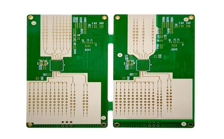
If you're looking for a reliable surface finish for multi-layer PCBs that ensures strong interconnections and soldering performance, immersion tin might be the ideal choice. This blog dives deep into the best practices for using immersion tin on multi-layer PCBs, focusing on interconnection reliability, soldering techniques, via connections, and design tips for plated through-hole (PTH) soldering. We'll cover everything from the basics of immersion tin to actionable strategies for optimizing your PCB design and assembly process, ensuring long-lasting performance for your projects.
What is Immersion Tin and Why Use It for Multi-Layer PCBs?
Immersion tin is a surface finish applied to printed circuit boards (PCBs) through a chemical process that deposits a thin layer of tin onto the copper pads. This finish protects the copper from oxidation and provides a flat, solderable surface for component attachment. For multi-layer PCBs, which often have complex designs with numerous interconnections and vias, immersion tin offers several advantages.
First, it ensures excellent solderability, which is critical for reliable connections in dense multi-layer boards. Second, it’s a lead-free option, aligning with environmental regulations like RoHS. Lastly, immersion tin provides a cost-effective solution compared to other finishes like gold plating, making it popular in industries such as automotive and consumer electronics where reliability is paramount.
However, achieving optimal results with immersion tin on a multi-layer PCB requires careful attention to design, thickness specifications, and soldering practices. Let’s explore how to make the most of this surface finish.
Key Benefits of Immersion Tin for Multi-Layer PCB Interconnections
Multi-layer PCBs often feature intricate interconnection systems, including vias and PTHs, that demand a surface finish capable of maintaining signal integrity and mechanical strength. Immersion tin stands out for several reasons:
- Flat Surface for Soldering: The uniform, thin layer of tin (typically 0.8 to 1.2 micrometers as per IPC-4554 standards) creates a planar surface ideal for both surface mount technology (SMT) and through-hole components.
- Oxidation Resistance: Tin protects copper from oxidizing, ensuring long-term solderability even after storage.
- Compatibility with Fine-Pitch Components: The smooth finish supports precise soldering for high-density interconnections, common in multi-layer designs.
- Cost-Effectiveness: Compared to alternatives like ENIG (Electroless Nickel Immersion Gold), immersion tin is more affordable while still delivering reliable performance.
Despite these benefits, immersion tin has challenges, such as the risk of tin whiskers—tiny conductive filaments that can cause short circuits. Proper handling and design considerations can mitigate these risks, which we’ll cover later in this post.
Best Practices for Immersion Tin Thickness and Solder Joint Reliability
One of the most critical factors for soldering reliability in multi-layer PCBs with immersion tin is the thickness of the tin layer. According to industry standards like IPC-4554, the ideal thickness for immersion tin is between 0.8 and 1.2 micrometers. Why does this range matter?
A layer thinner than 0.8 micrometers may not provide enough protection against copper oxidation or ensure good solderability. On the other hand, a layer thicker than 1.2 micrometers increases the risk of intermetallic compound (IMC) formation during soldering, which can weaken joints over time. IMC growth between tin and copper can lead to brittle connections, reducing the lifespan of the PCB, especially in high-temperature environments.
To ensure reliability:
- Work with your PCB fabricator to monitor tin thickness using techniques like X-ray fluorescence (XRF) analysis.
- Store PCBs in a controlled environment to prevent excessive IMC growth before assembly.
- Follow strict soldering temperature profiles (e.g., peak reflow temperatures around 260°C for lead-free solder) to minimize thermal stress on the tin layer.
Optimizing Via Connections in Multi-Layer PCBs with Immersion Tin
Vias are the backbone of multi-layer PCB interconnections, allowing signals to travel between layers. Whether using through-hole vias, blind vias, or buried vias, the surface finish plays a crucial role in ensuring reliable connections. Immersion tin supports via reliability by providing a solderable surface inside plated through-holes (PTHs) and on surface pads.
Here are some best practices for via connections:
- Ensure Proper Plating: During PCB fabrication, confirm that the immersion tin process evenly coats the inside of vias. Uneven plating can lead to weak solder joints or signal loss, especially in high-frequency designs where impedance control is critical (e.g., maintaining 50 ohms for RF signals).
- Use Appropriate Via Sizes: For multi-layer PCBs, via diameters typically range from 0.2 to 0.6 mm, depending on the board thickness and layer count. Smaller vias reduce parasitic capacitance, improving signal speed (often exceeding 1 GHz in high-speed designs).
- Avoid Overheating During Soldering: Excessive heat can degrade the tin layer inside vias, leading to poor wetting and unreliable connections. Use a reflow profile with a gradual ramp-up to peak temperature.
By focusing on these factors, you can maintain robust via connections that support the complex routing of multi-layer PCBs.
PTH Soldering Techniques for Immersion Tin Multi-Layer PCBs
Plated through-hole (PTH) soldering remains a common method for attaching components to multi-layer PCBs, especially for connectors and high-power components that require mechanical strength. Immersion tin enhances PTH soldering by ensuring good wettability, but specific techniques are necessary for consistent results.
- Prepare the PCB Surface: Before soldering, clean the PCB to remove any contaminants that could interfere with tin wetting. Use isopropyl alcohol and a lint-free cloth for best results.
- Control Soldering Temperature: For lead-free soldering, maintain a tip temperature of 300-350°C for manual soldering or a reflow peak of 260°C. This prevents thermal damage to the tin layer and surrounding materials.
- Use Adequate Solder Volume: Ensure enough solder flows into the PTH to form a strong fillet, typically covering 75-100% of the hole height for reliability.
- Inspect Post-Soldering: After assembly, visually check for incomplete fillets or voids in the solder joint. X-ray inspection can help detect hidden defects in multi-layer boards.
Proper PTH soldering with immersion tin not only strengthens mechanical connections but also ensures electrical continuity across layers, which is vital for multi-layer PCB performance.
Multi-Layer PCB Design Tips for Immersion Tin Applications
Designing a multi-layer PCB with immersion tin requires careful planning to maximize interconnection reliability and soldering performance. Here are some practical design tips to consider:
- Optimize Pad Sizes: For SMT components, follow IPC-7351 standards for pad dimensions to ensure proper solder wetting with immersion tin. For example, a 0603 resistor typically requires pads of 0.8 mm x 1.0 mm.
- Minimize Thermal Stress: Place thermal reliefs around PTH pads to reduce heat dissipation during soldering, preventing damage to the tin layer. A typical thermal relief design includes four spokes connecting the pad to the copper plane.
- Control Layer Stack-Up: In multi-layer designs (e.g., 6-layer or 8-layer boards), balance the stack-up to avoid warping during reflow soldering. Warping can cause uneven solder joints and stress on vias.
- Mitigate Tin Whisker Risk: Space components and traces adequately to reduce the chance of short circuits from tin whiskers. A minimum spacing of 0.5 mm between critical conductors is often recommended.
These design considerations help ensure that immersion tin performs effectively, supporting both electrical and mechanical reliability in complex multi-layer PCBs.
Challenges of Immersion Tin and How to Overcome Them
While immersion tin offers many benefits for multi-layer PCBs, it’s not without challenges. Understanding these issues and implementing solutions can help you achieve consistent results.
- Tin Whiskers: These microscopic growths can form on the tin surface over time, especially under stress or high humidity. To reduce risk, store PCBs in a dry, temperature-controlled environment and consider conformal coating for added protection.
- Limited Shelf Life: Immersion tin has a shorter shelf life compared to other finishes, typically 6-12 months before solderability degrades. Plan your assembly timeline accordingly and avoid prolonged storage.
- IMC Formation: Intermetallic compounds can form at the tin-copper interface, especially under high temperatures. Limit exposure to multiple reflow cycles (ideally no more than 2-3) to minimize IMC growth.
By addressing these challenges, you can maintain the reliability of immersion tin in demanding multi-layer PCB applications.
Conclusion: Achieving Reliability with Immersion Tin on Multi-Layer PCBs
Immersion tin is a versatile and cost-effective surface finish for multi-layer PCBs, offering excellent solderability and protection for complex interconnections. By following best practices—such as controlling tin thickness, optimizing via and PTH soldering techniques, and adhering to thoughtful design principles—you can ensure reliable performance in your PCB projects.
From maintaining signal integrity in high-speed vias to ensuring strong mechanical connections with PTH components, immersion tin supports the demands of modern multi-layer PCB designs. With careful attention to fabrication, assembly, and storage, this surface finish can help you achieve long-lasting soldering reliability and interconnection strength.
Whether you’re working on automotive electronics, industrial controls, or consumer devices, immersion tin provides a solid foundation for your multi-layer PCB needs. Implement these strategies in your next project to see the difference in quality and performance.
 ALLPCB


