ALLPCB


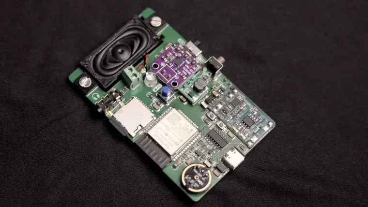
If you're an electrical engineer working on smart home devices, you might be wondering, "What are the key considerations for designing a PCB for voice assistants?" The answer lies in focusing on critical aspects like microphone array layout, audio signal processing, noise reduction, and echo cancellation. In this detailed guide, we’ll break down these elements to help you create a high-performing PCB design for voice assistants that meets the demands of modern smart home technology.
Voice assistants like Amazon Alexa, Google Assistant, and Apple Siri have become integral to smart homes, and their performance heavily relies on well-designed printed circuit boards (PCBs). Whether you're optimizing for clear voice capture or minimizing background noise, a thoughtful PCB design for voice assistants can make or break the user experience. Let’s dive into the specifics to ensure your design stands out.
Why PCB Design Matters for Voice Assistants
Voice assistants depend on precise audio input and output to function effectively. A poorly designed PCB can lead to issues like distorted voice commands, missed triggers, or excessive noise interference. For electrical engineers, the challenge is to balance compactness, power efficiency, and audio quality in a single board. A robust PCB design for voice assistants ensures seamless integration of hardware components, such as microphones, processors, and speakers, while maintaining signal integrity.
In the following sections, we’ll explore the core considerations for designing a PCB tailored for voice assistants, including microphone array PCB layout, audio signal processing PCB techniques, noise reduction PCB strategies, and echo cancellation PCB implementations. These elements are crucial for achieving high-quality voice recognition and user satisfaction in smart home devices.
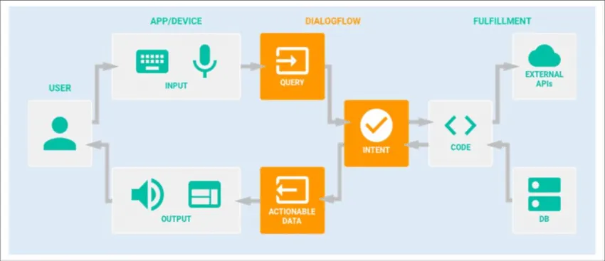
1. Microphone Array PCB Layout: Capturing Clear Voice Input
The microphone array is the heart of any voice assistant, as it captures user commands. Designing a microphone array PCB requires careful planning to ensure optimal sound capture from various directions while minimizing interference. Here are the key factors to consider:
- Placement and Spacing: Position microphones in a circular or linear array to enable beamforming, a technique that focuses on sound from specific directions. For example, a common setup for smart speakers uses 6-8 microphones spaced 40-50 mm apart to cover a 360-degree field. Incorrect spacing can lead to poor directional accuracy.
- Signal Integrity: Keep traces short between microphones and the preamplifier to avoid signal loss. Use a ground plane to shield against electromagnetic interference (EMI), which can distort audio input at frequencies around 2.4 GHz (common for Wi-Fi in smart homes).
- Power Supply Isolation: Microphones are sensitive to power supply noise. Dedicate separate power traces or use low-dropout regulators (LDOs) with a noise level below 10 μV RMS to ensure clean power delivery.
For engineers, testing the microphone array layout with simulation tools like Altium Designer or Cadence can help predict performance before fabrication. A well-designed microphone array PCB ensures voice assistants pick up commands accurately, even in noisy environments.
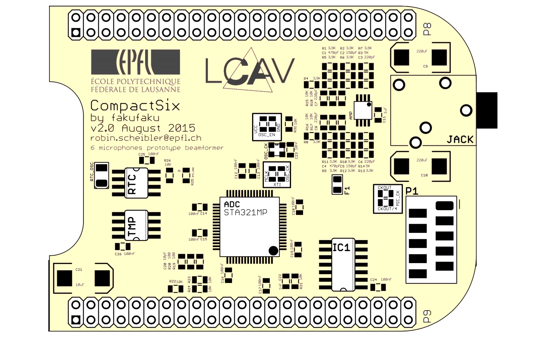
2. Audio Signal Processing PCB: Ensuring High-Quality Sound
Once the microphone array captures sound, the audio signal must be processed to filter out noise and enhance clarity. This is where an optimized audio signal processing PCB comes into play. The goal is to maintain signal fidelity while integrating digital signal processors (DSPs) or microcontrollers (MCUs) for real-time processing. Consider these design tips:
- Component Selection: Choose a DSP or MCU with sufficient processing power for audio algorithms. For instance, a processor like the Texas Instruments C5000 series can handle sample rates up to 48 kHz, which is ideal for voice recognition.
- Controlled Impedance: Audio signals are sensitive to impedance mismatches. Design traces with a characteristic impedance of 50-75 ohms for analog audio lines to prevent reflections and signal degradation.
- Analog-to-Digital Conversion (ADC): Place high-quality ADCs close to the microphone preamps to minimize noise pickup during conversion. Aim for a signal-to-noise ratio (SNR) of at least 80 dB to ensure clear digital output.
Additionally, ensure that the PCB layout separates analog and digital sections to avoid crosstalk. For example, place a ground plane split between analog audio components and digital processors to reduce interference. A well-executed audio signal processing PCB design guarantees that voice commands are processed accurately, even under challenging conditions.
3. Noise Reduction PCB Techniques: Minimizing Interference
Background noise is a major hurdle for voice assistants, especially in busy households. Designing a noise reduction PCB involves both hardware and layout strategies to suppress unwanted sounds and EMI. Here’s how to tackle noise effectively:
- Grounding and Shielding: Use a multi-layer PCB with a dedicated ground plane to shield sensitive audio circuits. For instance, a 4-layer board with a ground layer beneath the audio traces can reduce EMI by up to 20 dB compared to a 2-layer board.
- Filtering Components: Integrate low-pass filters with a cutoff frequency of around 8 kHz near the microphone inputs to block high-frequency noise from nearby Wi-Fi or Bluetooth modules operating at 2.4 GHz.
- Trace Routing: Route audio traces away from high-speed digital lines (like SPI or I2C buses) to prevent crosstalk. Maintain at least a 3x trace-width distance between audio and digital signals as a rule of thumb.
Noise reduction isn’t just about hardware; it also ties into software algorithms running on the DSP. However, a solid noise reduction PCB layout minimizes the burden on software by ensuring cleaner raw input. Engineers can test noise performance using spectrum analyzers to identify and mitigate interference sources during the design phase.
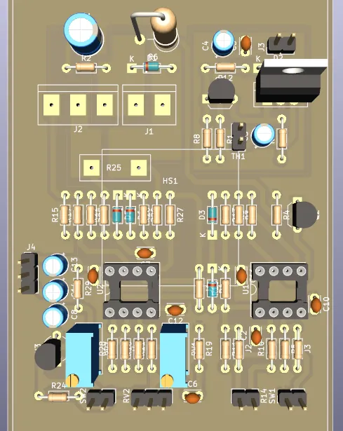
4. Echo Cancellation PCB Design: Eliminating Feedback Loops
Voice assistants often play audio through speakers while listening for commands, which can create echo or feedback loops. A well-designed echo cancellation PCB supports hardware-based solutions to complement software algorithms. Here are the critical design considerations:
- Separation of Audio Paths: Physically separate microphone and speaker traces on the PCB to reduce direct coupling. For example, route speaker output traces on the bottom layer and microphone input traces on the top layer of a multi-layer board.
- Reference Signal Path: Provide a clean reference signal from the speaker output to the echo cancellation circuitry. This allows the DSP to subtract the played audio from the microphone input. Use matched trace lengths to avoid timing mismatches, aiming for delays under 1 ms.
- High-Quality Components: Use op-amps with a slew rate of at least 10 V/μs in the echo cancellation circuit to handle rapid signal changes without distortion.
Echo cancellation is a complex interplay of hardware and software, but a robust echo cancellation PCB design lays the foundation for effective performance. Testing with real-world scenarios, such as playing music at 80 dB while speaking commands, can validate the design before mass production.
5. Power Management and Thermal Considerations
Voice assistants operate continuously, so power efficiency and thermal management are vital in PCB design. Here’s how to address these aspects:
- Power Supply Design: Use switching regulators with efficiencies above 85% to minimize power loss. For sensitive audio circuits, add LDOs to provide clean voltage with ripple below 10 mV.
- Thermal Dissipation: Place heat-generating components like DSPs or power ICs near thermal vias or heat sinks. Ensure a thermal resistance below 50°C/W to keep junction temperatures under 85°C during operation.
- Low-Power Modes: Design the PCB to support sleep modes for components like microphones and processors, reducing power draw to under 10 mW when idle.
Efficient power management not only extends the lifespan of the device but also ensures consistent performance, which is critical for always-on voice assistants.
6. Testing and Validation for Optimal Performance
Before finalizing your PCB design, thorough testing is essential to ensure reliability. Use these strategies to validate your PCB design for voice assistants:
- Audio Quality Tests: Measure SNR and total harmonic distortion (THD) using audio analyzers. Aim for an SNR above 80 dB and THD below 0.1% for clear voice capture.
- Environmental Testing: Test the device in noisy environments (e.g., 60 dB background noise) to evaluate noise reduction and echo cancellation performance.
- EMI Compliance: Use an EMI test chamber to ensure the PCB meets FCC or CE standards for radiated emissions, especially in the 2.4 GHz band used by Wi-Fi.
Iterative testing and refinement can catch issues early, saving time and cost in later stages of development.
Conclusion: Building the Future of Smart Home Voice Assistants
Designing a PCB for voice assistants is a complex but rewarding task for electrical engineers. By focusing on microphone array PCB layout, audio signal processing PCB optimization, noise reduction PCB techniques, and echo cancellation PCB strategies, you can create a board that delivers exceptional audio performance in smart home devices. Add in proper power management and rigorous testing, and you’re well on your way to building a voice assistant that users will love.
Remember, every detail counts—from the spacing of microphones to the routing of traces. Use simulation tools, adhere to best practices, and test relentlessly to ensure your PCB design for voice assistants meets the high standards of today’s smart home market. Have you worked on a voice assistant PCB before? Share your challenges and solutions in the comments—we’d love to hear your insights!