 ALLPCB


High-Density Interconnect (HDI) PCBs are at the forefront of modern electronics, enabling smaller, faster, and more complex designs. However, with increased density comes the challenge of maintaining signal integrity. If you're searching for solutions to HDI PCB signal integrity issues, looking into signal integrity analysis for HDI PCB, or tackling crosstalk in HDI PCBs, this guide offers a clear starting point. Signal integrity problems in HDI PCBs often stem from tight spacing, high-speed signals, and layered designs, leading to issues like crosstalk, impedance mismatches, and signal delays. The good news? These challenges can be identified and mitigated with the right strategies, such as proper stack-up design, controlled impedance, and advanced simulation tools.
In this comprehensive blog, we dive deep into the causes of signal integrity issues in HDI PCBs, explore analysis techniques, and provide actionable mitigation strategies to ensure your designs perform reliably. Whether you're an engineer working on cutting-edge devices or a designer aiming for optimal performance, this post will equip you with the knowledge to overcome these challenges.
What Are HDI PCBs and Why Do They Face Signal Integrity Challenges?
HDI PCBs are specialized circuit boards designed with a higher wiring density than traditional PCBs. They use microvias, fine traces, and multiple layers to pack more functionality into a smaller footprint. This makes them ideal for applications like smartphones, medical devices, and high-speed communication systems. However, the very features that make HDI PCBs powerful—such as trace widths as narrow as 3 mils (0.003 inches) and via diameters below 6 mils—also create unique challenges for maintaining signal integrity.
Signal integrity refers to the ability of a signal to travel from its source to its destination without distortion or loss. In HDI PCBs, the close proximity of traces, high layer counts (often exceeding 10 layers), and high-frequency signals (sometimes over 5 GHz) increase the risk of interference and degradation. Common issues include crosstalk, where signals from adjacent traces interfere with each other, and impedance mismatches, which can cause signal reflections and delays. Understanding these challenges is the first step toward addressing them effectively.
Key Signal Integrity Issues in HDI PCBs
Let’s break down the primary signal integrity challenges that engineers face when designing and manufacturing HDI PCBs. Identifying these issues early can save time and prevent costly redesigns.
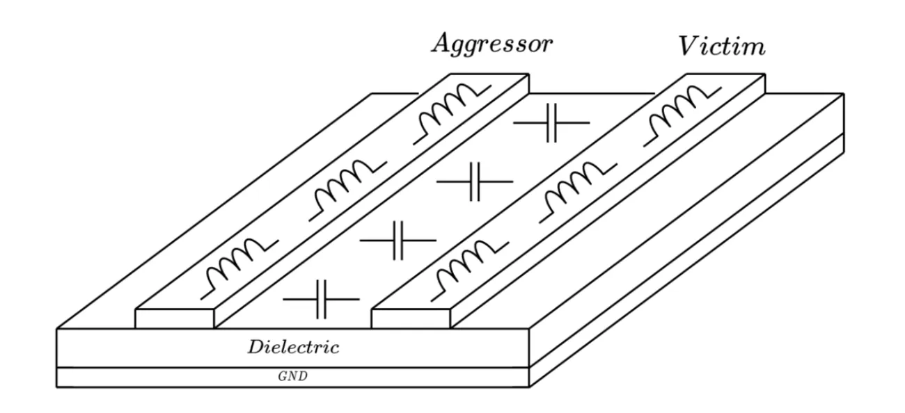
1. Crosstalk in HDI PCBs
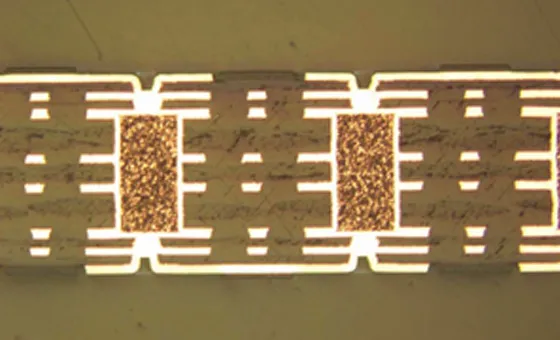
Crosstalk occurs when a signal from one trace interferes with a neighboring trace, causing noise and potential data errors. In HDI PCBs, traces are often spaced less than 5 mils apart, amplifying the risk of electromagnetic coupling. At high frequencies, such as those above 1 GHz, this interference can significantly degrade performance, especially in applications like telecommunications or data centers.
For example, in a 12-layer HDI PCB with a signal speed of 2.5 GHz, crosstalk can introduce noise levels as high as 10% of the original signal amplitude if not properly managed. This can lead to bit errors in digital systems, disrupting overall functionality.
2. Impedance Mismatches
Impedance mismatches happen when the characteristic impedance of a trace doesn’t align with the source or load impedance, causing signal reflections. In HDI PCBs, maintaining consistent impedance (often targeted at 50 ohms for high-speed signals) is tricky due to varying dielectric materials, trace widths, and layer transitions. A mismatch as small as 10% can result in a reflection coefficient of 0.05, leading to signal loss and timing issues.
3. Signal Delay and Skew
Signal delay and skew refer to timing differences between signals traveling through different paths on the PCB. In HDI designs with multiple layers and microvias, signals may take slightly different routes, causing delays. For instance, a delay of just 100 picoseconds in a 5 GHz signal can shift the phase by 180 degrees, potentially causing data misalignment in high-speed systems.
4. Power Integrity and Noise
Power integrity issues, such as voltage drops or ground bounce, can also affect signal quality in HDI PCBs. With high-density designs, power and ground planes are often fragmented, leading to insufficient decoupling and noise on the power supply lines. This noise can couple into signal traces, especially in designs operating at voltages as low as 1.2V, common in modern electronics.
Signal Integrity Analysis for HDI PCB Designs
Before diving into solutions, it’s critical to analyze and identify signal integrity issues during the design phase. Signal integrity analysis for HDI PCB involves using specialized tools and techniques to predict and measure potential problems. Here are the key steps and methods to perform this analysis effectively.
1. Pre-Layout Simulation
Pre-layout simulation uses software to model signal behavior based on the PCB’s proposed design. Tools can simulate impedance, crosstalk, and signal delays by inputting parameters like trace width (e.g., 4 mils), spacing (e.g., 5 mils), and dielectric constant (typically 4.2 for FR-4 material). This step helps identify potential issues before physical prototyping, saving time and cost.
2. Post-Layout Analysis
Once the layout is complete, post-layout analysis verifies the design by extracting the actual trace geometries and via structures. This process can detect impedance discontinuities caused by microvia transitions or inconsistent trace routing. For example, a sudden change in trace width from 4 mils to 6 mils can cause a 5-ohm impedance shift, which post-layout tools can flag for correction.
3. Time-Domain Reflectometry (TDR)
TDR is a measurement technique used to locate impedance mismatches in a fabricated HDI PCB. By sending a fast pulse down a trace and measuring the reflected signal, TDR can pinpoint discontinuities with a resolution of less than 1 inch. This is particularly useful for validating high-speed designs where even small mismatches matter.
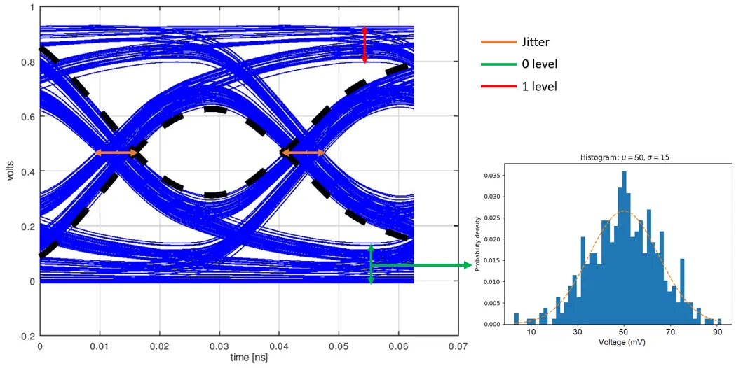
4. Eye Diagram Testing
Eye diagram testing evaluates the quality of digital signals by overlaying multiple signal transitions. A “closed” eye indicates noise or timing issues, while an “open” eye suggests good signal integrity. For HDI PCBs handling data rates above 2.5 Gbps, eye diagram testing is essential to ensure reliable communication.
Mitigation Strategies for HDI PCB Signal Integrity Issues
Now that we’ve identified the challenges and analysis methods, let’s explore practical strategies to mitigate HDI PCB signal integrity issues. These solutions can be applied during design, layout, and manufacturing stages to ensure optimal performance.
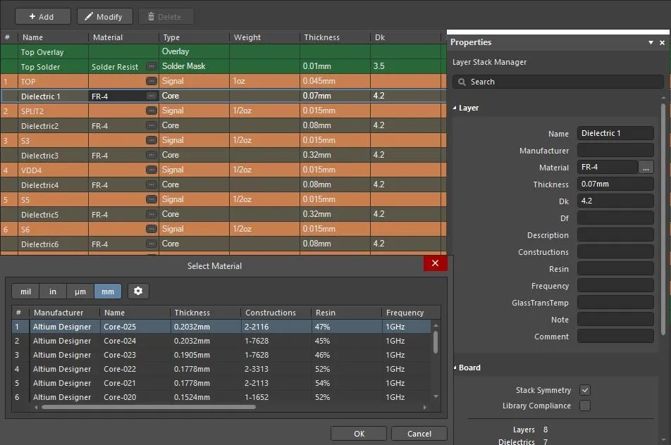
1. Optimize PCB Stack-Up Design
A well-planned stack-up is the foundation of signal integrity. Place high-speed signal layers between solid ground planes to create a controlled impedance environment and reduce crosstalk. For example, in an 8-layer HDI PCB, dedicate layers 2 and 6 as ground planes to shield signal layers 3 and 5. Additionally, use thin dielectric materials (e.g., 4 mils thick) between layers to minimize via stub effects.
2. Control Trace Spacing and Width
To reduce crosstalk in HDI PCBs, maintain adequate spacing between traces, ideally at least 3 times the trace width. For a 4-mil trace, aim for a 12-mil separation where possible. If space constraints prevent this, route high-speed signals on different layers or use differential pairs to cancel out noise. Also, ensure consistent trace widths to avoid impedance mismatches.
3. Use Microvias Strategically
Microvias, while essential for HDI designs, can introduce signal degradation if not used correctly. Minimize via stubs—unused portions of vias that act as antennas for noise—by using back-drilling or designing blind and buried vias. For high-speed signals above 3 GHz, keep via transitions to a minimum, as each transition can cause a 2-3% signal loss.
4. Implement Proper Grounding
A solid grounding strategy is crucial for reducing noise and ensuring power integrity. Use continuous ground planes wherever possible, and avoid splitting ground planes under high-speed traces. Place decoupling capacitors (e.g., 0.1 μF) close to power pins of ICs to filter out noise, ensuring a stable voltage supply even at high frequencies.
5. Leverage Differential Signaling
For high-speed data transmission, differential signaling is a powerful technique to combat crosstalk and noise. By sending complementary signals on paired traces, interference affects both lines equally and can be canceled out at the receiver. This approach is especially effective in HDI PCBs handling data rates above 1 Gbps.
6. Use Advanced Materials
Standard FR-4 material may not suffice for high-frequency HDI designs due to its higher dielectric loss. Consider low-loss materials like Rogers 4350B, which has a dielectric constant of 3.48 and a loss tangent of 0.0037 at 10 GHz, compared to FR-4’s loss tangent of 0.02. These materials help maintain signal integrity at frequencies above 5 GHz.
Manufacturing Considerations for Signal Integrity in HDI PCBs
Even the best design can fail if manufacturing processes aren’t aligned with signal integrity goals. During production, ensure tight control over trace etching to maintain widths within ±10% of the design value. For instance, a 4-mil trace should not vary beyond 0.4 mils to avoid impedance shifts. Additionally, verify dielectric thickness consistency, as a variation of just 0.5 mils can alter impedance by 2-3 ohms.
Work closely with your manufacturing partner to validate microvia reliability through cross-sectional analysis and thermal testing. Poorly formed microvias can cause signal discontinuities, especially under thermal stress. Finally, request post-fabrication testing, such as TDR measurements, to confirm that the board meets impedance and signal quality specifications.
Conclusion: Mastering Signal Integrity in HDI PCBs
Signal integrity challenges in HDI PCBs, such as crosstalk in HDI PCBs, impedance mismatches, and signal delays, are inevitable due to the compact and complex nature of these designs. However, with thorough signal integrity analysis for HDI PCB and proven mitigation strategies, these issues can be effectively managed. From optimizing stack-up designs and trace spacing to leveraging advanced materials and manufacturing precision, engineers have a robust toolkit to ensure reliable performance.
By addressing HDI PCB signal integrity issues early in the design process and collaborating with experienced manufacturing teams, you can create high-performing boards for even the most demanding applications. Whether you're designing for telecommunications, medical devices, or consumer electronics, mastering signal integrity will set your projects apart in terms of quality and reliability.


