ALLPCB


In the world of printed circuit board (PCB) manufacturing, choosing the right lamination process can make or break your project. If you're wondering whether to use sequential lamination or conventional lamination, the answer depends on your design needs, budget, and performance goals. Sequential lamination is often ideal for high-density interconnect (HDI) boards, offering better space efficiency and signal integrity, while conventional lamination suits simpler, cost-sensitive designs with fewer layers. In this comprehensive guide, we'll dive deep into the differences, exploring sequential lamination advantages, conventional lamination disadvantages, and a detailed PCB manufacturing cost comparison to help you make an informed decision.
What Is PCB Lamination and Why Does It Matter?
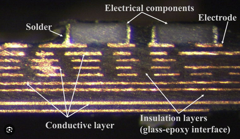
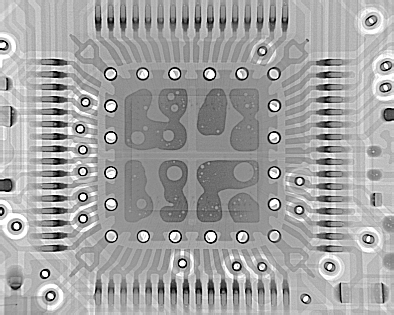
PCB lamination is a critical step in manufacturing where layers of copper and insulating materials, like prepreg and core, are bonded together under heat and pressure to form a solid, multilayer board. This process directly impacts the board's durability, electrical performance, and overall cost. Whether you're designing a simple two-layer board for a basic gadget or a complex HDI board for a smartphone, the lamination method you choose affects everything from signal speed to manufacturing time.
Two primary methods dominate the industry: sequential lamination and conventional lamination. Each has unique strengths and weaknesses, which we'll explore in detail to help you pick the right process for your next project.

Understanding Conventional Lamination: The Traditional Approach
Conventional lamination, often called simultaneous lamination, is the traditional method used in PCB manufacturing. In this process, all layers of the PCB—copper foils, prepreg, and core materials—are stacked together and laminated in a single step under high heat (around 180-200°C) and pressure (typically 300-500 psi). This bonds the materials into a unified structure, ready for drilling and plating.
Advantages of Conventional Lamination
- Simplicity: Since all layers are laminated at once, the process is straightforward and requires fewer manufacturing steps. This makes it ideal for simpler designs with 2-6 layers.
- Cost-Effective for Low-Layer Boards: With fewer cycles of lamination, production time and costs are lower for basic designs. For example, a 4-layer board using conventional lamination might cost 20-30% less than an HDI board with sequential lamination.
- Widely Available: Most manufacturing facilities are equipped for conventional lamination, making it a go-to option for standard projects.
Conventional Lamination Disadvantages
While conventional lamination works well for basic designs, it falls short in more advanced applications. Here are some key drawbacks:
- Limited Layer Density: This method struggles with high-layer-count boards (8+ layers) and HDI designs. It can't easily accommodate blind or buried vias, which are essential for compact, high-performance electronics.
- Poor Signal Integrity for High-Speed Designs: In high-frequency applications, signal integrity is crucial. Conventional lamination often leads to longer signal paths and higher impedance mismatches, with values potentially deviating by 10-15% from design specs, affecting performance at speeds above 1 GHz.
- Material Stress: Laminating all layers at once can cause uneven stress distribution, leading to warpage or delamination over time, especially in boards larger than 12x12 inches.
- Scalability Issues: As designs become more complex, the single-step process becomes less practical, increasing defect rates by up to 5-10% in boards with more than 10 layers.
Conventional lamination is best for cost-sensitive projects with minimal complexity, but it may not meet the needs of modern, high-performance electronics.

Exploring Sequential Lamination: The Modern Solution for HDI
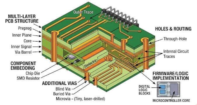
Sequential lamination is a more advanced technique, often used for HDI PCBs. Unlike conventional lamination, this process builds the board in stages. It starts with a core layer, laminates additional layers on top in multiple cycles, and incorporates blind and buried vias at each stage. Each lamination cycle typically occurs at temperatures of 170-190°C and pressures of 200-400 psi, ensuring precise alignment and bonding.
Sequential Lamination Advantages
For engineers working on cutting-edge designs, sequential lamination offers several compelling benefits:
- Support for HDI Designs: This method enables the creation of blind and buried vias, allowing for denser component placement. For instance, HDI boards using sequential lamination can achieve via diameters as small as 0.1 mm, compared to 0.3 mm in conventional processes.
- Improved Signal Integrity: Shorter signal paths and precise impedance control (within ±5% of target values) make this process ideal for high-speed applications, supporting data rates up to 10 Gbps or higher.
- Greater Design Flexibility: Sequential lamination allows for complex multilayer structures (up to 20+ layers) without sacrificing reliability, making it perfect for compact devices like wearables and IoT gadgets.
- Reduced Warpage: By laminating in stages, stress is distributed more evenly, reducing warpage risks by up to 30% compared to conventional methods, especially in larger boards.
Challenges of Sequential Lamination
Despite its advantages, sequential lamination isn't without drawbacks:
- Higher Costs: Multiple lamination cycles mean longer production times and higher costs. A 10-layer HDI board using sequential lamination might cost 40-60% more than a similar board made with conventional lamination.
- Complex Manufacturing: The process requires advanced equipment and skilled technicians, which may not be available at all facilities.
- Longer Lead Times: Each lamination cycle adds time to production, potentially extending lead times by 3-5 days for complex designs.
Sequential lamination shines in applications where performance and density are priorities, but it demands a higher budget and careful planning.

PCB Manufacturing Cost Comparison: Breaking Down the Numbers
Cost is often a deciding factor when choosing between sequential and conventional lamination. Let's compare the two processes across key factors to give you a clearer picture.
Material Costs
Both methods use similar materials like copper foil, prepreg, and core substrates, but sequential lamination often requires higher-grade materials to maintain precision in HDI designs. For a 6-layer board, material costs might be roughly $0.50 per square inch for conventional lamination, while sequential lamination could push this to $0.70-$0.90 per square inch due to tighter tolerances and additional via-fill materials.
Labor and Equipment Costs
Conventional lamination is less labor-intensive, as it involves a single cycle. Labor costs for a standard 4-layer board might be around $1.00-$1.50 per square inch. Sequential lamination, with its multiple cycles, can increase labor costs to $2.00-$3.00 per square inch, reflecting the need for skilled operators and specialized equipment.
Production Time and Yield
Time is money in PCB manufacturing. Conventional lamination typically takes 1-2 days for a 4-6 layer board, while sequential lamination might take 3-5 days due to additional cycles. Yield rates also differ—conventional processes may have a defect rate of 2-5% for simpler boards, while sequential lamination, though more precise, can see slightly higher defect rates (3-7%) in complex designs due to alignment challenges.
Total Cost Estimate
For a small batch of 100 units of a 4x4 inch, 6-layer board:
- Conventional Lamination: Approximately $800-$1,200 total, or $8-$12 per board, factoring in materials, labor, and overhead.
- Sequential Lamination: Approximately $1,200-$1,800 total, or $12-$18 per board, reflecting higher material and labor costs.
These numbers are rough estimates and can vary based on design complexity, volume, and facility capabilities. For high-volume production, economies of scale may reduce costs for both methods, but sequential lamination often remains pricier.
Key Factors to Consider When Choosing a Lamination Process
With the technical and cost differences laid out, here are the main factors to weigh when deciding between sequential and conventional lamination:
- Design Complexity: If your project involves HDI features, blind/buried vias, or more than 8 layers, sequential lamination is likely the better choice. For simpler 2-6 layer boards, conventional lamination suffices.
- Performance Needs: High-speed or high-frequency designs (above 1 GHz) benefit from sequential lamination's superior signal integrity. For low-speed applications, conventional methods are adequate.
- Budget Constraints: If cost is a primary concern and your design is straightforward, stick with conventional lamination to save 20-40% on production costs.
- Production Volume: For prototypes or low-volume runs, the higher cost of sequential lamination might be justifiable if performance is critical. For mass production of basic boards, conventional lamination offers better savings.
- Lead Time: If you're on a tight schedule, conventional lamination's shorter production time could be a deciding factor.
Real-World Applications: When to Use Each Method
To bring this comparison to life, let's look at typical scenarios where each lamination process excels.
Conventional Lamination Use Cases
- Consumer Electronics: Simple devices like basic remote controls or LED lighting boards often use 2-4 layers and don't require HDI features. Conventional lamination keeps costs low.
- Prototyping: For early-stage prototypes where performance isn't critical, conventional lamination offers a quick, affordable way to test designs.
Sequential Lamination Use Cases
- Mobile Devices: Smartphones and tablets rely on HDI boards with 10+ layers and microvias for compact, high-performance designs. Sequential lamination is essential here.
- Automotive Electronics: Modern vehicles use complex PCBs for sensors and control systems, often requiring precise impedance control and high reliability, which sequential lamination supports.
- Medical Devices: Equipment like wearable health monitors needs dense, reliable boards to handle sensitive signals, making sequential lamination the preferred choice.
Tips for Optimizing Your PCB Lamination Process
Regardless of the method you choose, here are some practical tips to ensure a smooth manufacturing process:
- Work Closely with Your Manufacturer: Share detailed design files and discuss your performance and budget needs to select the best lamination method.
- Minimize Layer Count When Possible: Reducing layers can lower costs, especially with conventional lamination, without compromising functionality in simpler designs.
- Plan for Testing: Allocate time and budget for testing signal integrity and thermal performance, especially for HDI boards using sequential lamination.
- Consider Material Selection: Choose materials with compatible thermal expansion coefficients to reduce stress and warpage during lamination.
Conclusion: Making the Right Choice for Your PCB Project
Choosing between sequential lamination and conventional lamination comes down to balancing performance, complexity, and cost. Sequential lamination offers unmatched advantages for HDI and high-speed designs, with superior signal integrity and design flexibility, but it comes at a higher price. Conventional lamination, while limited in scope, remains a cost-effective solution for simpler boards with fewer layers.
By understanding the sequential lamination advantages, acknowledging the conventional lamination disadvantages, and carefully reviewing a PCB manufacturing cost comparison, you can select the process that aligns with your project's goals. Whether you're designing a cutting-edge wearable or a basic control board, the right lamination method ensures reliability and performance without breaking the bank.