 ALLPCB


In the fast-paced world of electronics, high-speed printed circuit boards (PCBs) are at the heart of modern devices, from smartphones to data centers. One critical factor in ensuring these boards perform reliably is power plane impedance control. But what exactly is it, and why does it matter? Simply put, power plane impedance control involves designing the power distribution network on a PCB to minimize noise and maintain signal integrity in high-speed design. Without proper control, signals can distort, leading to errors or system failures.
In this comprehensive guide, we’ll dive deep into the concept of controlled impedance PCB design, focusing on power planes and their role in achieving clean, reliable signals. Whether you’re an engineer working on cutting-edge technology or a designer looking to optimize your next project, this blog will provide actionable insights into impedance matching and power plane strategies for high-speed PCBs.
What Is Power Plane Impedance and Why Does It Matter?
Before we explore the details, let’s break down the basics. A power plane in a PCB is a large, continuous layer of copper that delivers power to various components. Its impedance—the resistance to the flow of alternating current (AC)—plays a huge role in how well the power is distributed. Low impedance in the power plane ensures that components receive stable voltage, even when current demands spike during high-speed operations.
In high-speed design, signals switch at incredibly fast rates, often in the gigahertz range. Without proper power plane impedance control, these rapid changes can cause noise, voltage drops, or electromagnetic interference (EMI), all of which degrade signal integrity. For instance, a poorly designed power plane might lead to a voltage ripple of 100 mV or more, which can disrupt sensitive circuits operating at 1.2V.
By maintaining a controlled impedance PCB, designers can reduce these risks, ensuring that signals remain clear and data transfer is error-free. This is especially critical in applications like 5G communication, automotive radar, and high-performance computing.
The Role of Power Planes in Signal Integrity
Signal integrity refers to the quality of an electrical signal as it travels through a PCB. In high-speed systems, even small distortions can cause data loss or timing errors. Power planes are key to maintaining signal integrity because they act as a stable reference for signals and help manage noise.
Here’s how power planes impact signal integrity:
- Noise Reduction: A well-designed power plane minimizes voltage fluctuations, reducing noise that can interfere with signals.
- Return Path: Power planes often work with ground planes to provide a low-impedance return path for high-speed signals, preventing signal distortion.
- Decoupling: Power planes, when paired with decoupling capacitors, help filter out high-frequency noise, ensuring clean power delivery.
For example, in a PCB handling 10 Gbps data rates, improper power plane design could introduce jitter—random variations in signal timing—exceeding 10 picoseconds, which is enough to cause bit errors. Controlling power plane impedance keeps such issues in check.
Understanding Controlled Impedance in PCB Design
A controlled impedance PCB is designed to maintain specific impedance values for traces, power planes, and ground planes. While controlled impedance often focuses on signal traces, the impedance of power planes is equally important in high-speed designs.
Impedance in power planes is influenced by several factors:
- Plane Thickness: Thicker copper layers reduce resistance and lower impedance.
- Dielectric Material: The material between power and ground planes affects capacitance and, therefore, impedance. Materials with a high dielectric constant (like FR-4 at 4.2) increase capacitance, lowering impedance at high frequencies.
- Plane Spacing: Closer spacing between power and ground planes increases capacitance, reducing impedance.
For instance, reducing the spacing between a power plane and ground plane from 10 mils to 5 mils can double the capacitance, significantly lowering impedance at frequencies above 100 MHz. This helps stabilize power delivery during rapid signal switching.
Impedance Matching Techniques for Power Planes
Impedance matching isn’t just for signal traces—it’s also vital for power planes in high-speed PCBs. The goal is to ensure that the power delivery network (PDN) has low impedance across a wide range of frequencies, preventing voltage drops and noise.
Here are some practical techniques for achieving impedance matching in power planes:
- Use Thin Dielectric Layers: As mentioned earlier, closer spacing between power and ground planes lowers impedance. Aim for dielectric thicknesses below 5 mils for high-speed designs if possible.
- Place Decoupling Capacitors Strategically: Capacitors act as local energy storage, smoothing out voltage spikes. Place them close to high-speed components, targeting a range of capacitance values (e.g., 0.1 μF to 10 μF) to cover different frequency bands.
- Optimize Plane Geometry: Avoid splitting power planes unnecessarily, as splits can increase impedance and create noise. If splits are needed, ensure they don’t disrupt the return path for critical signals.
- Simulate the PDN: Use simulation tools to model the power plane’s impedance profile. Target an impedance below 1 ohm across frequencies from 1 kHz to 100 MHz to ensure stable power delivery.
By applying these techniques, you can maintain a low-impedance PDN, which is crucial for signal integrity in high-speed design. For example, a well-matched power plane can reduce voltage noise by up to 50%, directly improving signal quality.
Challenges in Power Plane Impedance Control
While controlling power plane impedance sounds straightforward, it comes with challenges, especially in complex, multilayer PCBs used for high-speed applications.
- Frequency-Dependent Behavior: Impedance varies with frequency. At low frequencies, resistance dominates, while at high frequencies, inductance and capacitance take over. Designers must balance these effects across the operating range.
- Component Density: High-density designs leave little room for wide power planes or multiple decoupling capacitors, making impedance control harder.
- Manufacturing Tolerances: Variations in dielectric thickness or copper etching during fabrication can alter impedance. For instance, a 10% variation in dielectric thickness can shift impedance by 5-10%, affecting performance.
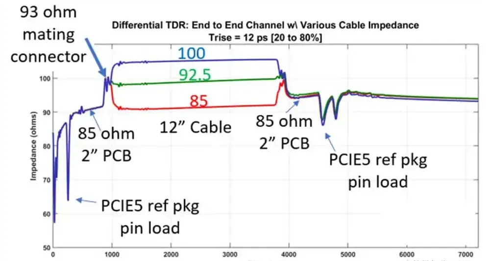
To overcome these challenges, work closely with your PCB manufacturer to define tight tolerances and validate designs through simulation and testing. Tools like time-domain reflectometry (TDR) can measure actual impedance after fabrication to ensure it matches the design target.
Best Practices for High-Speed PCB Design with Controlled Impedance
Designing a high-speed PCB with controlled impedance requires a holistic approach. Here are some best practices to ensure both power plane and signal trace impedance are optimized for signal integrity:
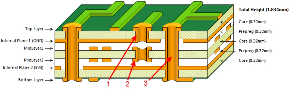
- Layer Stackup Planning: Design your stackup with alternating power and ground planes to maximize capacitance and minimize impedance. A common stackup for high-speed designs might include 8 layers, with power and ground planes sandwiching signal layers.
- Minimize Via Inductance: Vias connecting components to power planes introduce inductance, raising impedance. Use multiple vias or larger via sizes to reduce this effect.
- Route Signals Carefully: Keep high-speed signal traces short and avoid crossing power plane splits to maintain a consistent return path.
- Test and Iterate: After prototyping, test your PCB for impedance and noise using oscilloscopes or network analyzers. Adjust the design based on real-world data.
Following these practices can significantly improve the performance of your PCB. For example, a well-planned stackup can reduce power plane impedance by 20-30% compared to a poorly optimized layout, directly enhancing signal quality.
Tools and Technologies for Impedance Control
Modern PCB design tools make it easier to achieve controlled impedance in both signal traces and power planes. Here are some technologies and methods to consider:
- PDN Simulation Software: Tools that simulate power distribution networks can predict impedance across frequencies, helping you identify potential issues before fabrication.
- 3D Field Solvers: These tools calculate electromagnetic fields in your PCB, providing accurate impedance values for complex geometries.
- Fabrication Feedback: Collaborate with your PCB manufacturer to understand their capabilities and limitations. Many offer impedance testing services to verify your design after production.
Using these tools, you can fine-tune your design to meet strict impedance targets, such as maintaining a power plane impedance below 0.5 ohms up to 1 GHz for ultra-high-speed applications.
Conclusion: Mastering Power Plane Impedance for Reliable High-Speed PCBs
In the realm of high-speed design, every detail counts, and power plane impedance control is a cornerstone of achieving flawless signal integrity. By understanding the principles of controlled impedance PCB design and applying techniques like impedance matching, you can build boards that handle the demands of modern electronics with ease.
From optimizing plane spacing to using decoupling capacitors effectively, the strategies outlined in this guide offer a clear path to success. Whether you’re working on a 10 Gbps data link or a 5G communication module, controlling power plane impedance ensures your signals stay clean and your system performs reliably.
Start implementing these practices in your next project, and you’ll see the difference in performance and reliability. With the right approach, high-speed PCB design doesn’t have to be a challenge—it can be a competitive advantage.


