ALLPCB


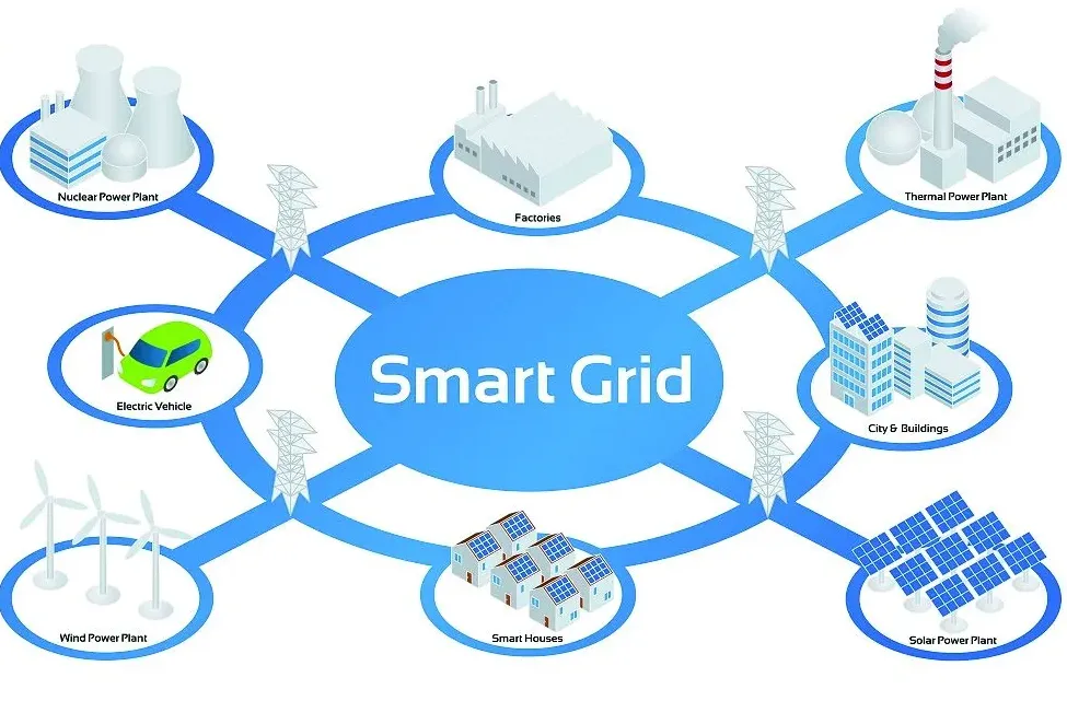
Smart grids are transforming the way we manage and distribute electricity, making power systems more efficient and reliable. At the heart of this revolution are Power Distribution PCBs (Printed Circuit Boards), which play a critical role in ensuring stable power delivery and minimal energy loss. If you're looking for solutions on power distribution in smart grids via PCBs, PCB design for high-power grids, or PCB layout for minimal energy loss in distribution, this guide will walk you through the essentials of designing PCBs that optimize power distribution systems and provide effective power distribution network PCB solutions.
In this comprehensive blog, we'll dive deep into the role of PCBs in smart grids, key design considerations, and best practices to achieve efficiency and reliability. Whether you're an engineer or a designer working on high-power systems, this post will provide actionable insights to help you succeed.
What Are Smart Grids and Why Do PCBs Matter?
Smart grids are modern electricity networks that use digital technology to monitor, control, and optimize the flow of power. Unlike traditional grids, they integrate renewable energy sources, real-time data, and automated systems to improve efficiency and reduce outages. In such complex systems, power distribution must be precise and reliable, and this is where PCBs come into play.
PCBs are the backbone of electronic devices and systems, including those used in smart grids. They manage the flow of electricity, control signals, and ensure that power is distributed evenly across components. For smart grids, PCBs that optimize power distribution systems are essential to handle high currents, minimize energy loss, and maintain stability under varying loads.
The Role of Power Distribution PCBs in Smart Grids
Power Distribution PCBs in smart grids are designed to handle high voltages and currents while ensuring minimal energy loss. They are used in various components such as inverters, converters, sensors, and control units that manage power flow. Here’s how they contribute:
- Efficient Power Delivery: PCBs ensure that power reaches every part of the grid without significant drops in voltage or current.
- Signal Integrity: They maintain clean and stable signals for communication between grid components, crucial for real-time monitoring.
- Thermal Management: High-power grids generate heat, and PCBs help dissipate it to prevent failures.
- Compact Design: PCBs allow for compact and scalable solutions, fitting into the tight spaces of smart grid equipment.
By focusing on power distribution network PCB solutions, engineers can create systems that are not only efficient but also durable and cost-effective.
Key Design Considerations for Power Distribution PCBs in High-Power Grids
Designing PCBs for smart grids, especially for high-power applications, requires careful planning. Below are the critical considerations to keep in mind when working on PCB design for high-power grids.
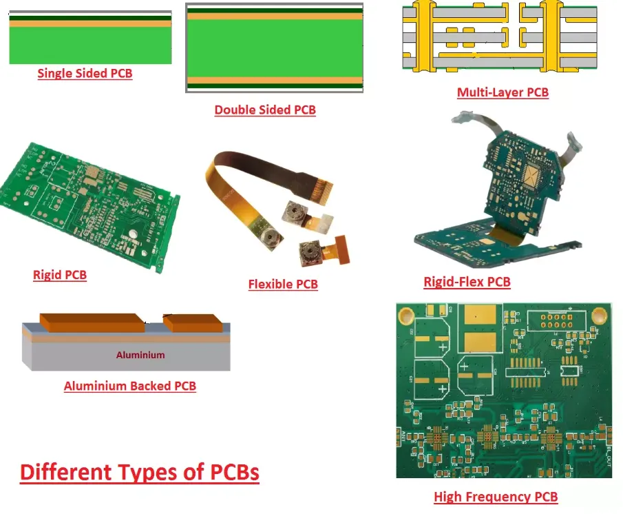
1. Material Selection for High-Power Handling
The choice of PCB material is vital for handling the high currents and voltages in smart grids. Standard FR-4 materials may not suffice for high-power applications due to their limited thermal conductivity and dielectric strength. Instead, consider:
- High-Tg Materials: These materials have a higher glass transition temperature, making them suitable for temperatures above 150°C often seen in power grids.
- Ceramic or Metal-Core PCBs: These offer better heat dissipation, with thermal conductivity values ranging from 1.5 to 9 W/mK compared to FR-4’s 0.3 W/mK.
Using the right material ensures the PCB can withstand the stress of high-power distribution without degrading over time.
2. Trace Width and Copper Thickness for Current Capacity
In high-power grids, traces must carry significant current without overheating or causing voltage drops. The width and thickness of copper traces are key factors:
- Trace Width: For a current of 10A, a trace width of at least 100 mils (2.54 mm) is recommended on a 1 oz copper PCB to keep temperature rise below 10°C.
- Copper Thickness: Opt for 2 oz or 3 oz copper (70-105 μm) instead of the standard 1 oz (35 μm) to handle higher currents and reduce resistance.
Using online calculators or design software can help determine the exact trace width and thickness based on current and temperature constraints, ensuring minimal energy loss in distribution.
3. Power and Ground Planes for Stability
Incorporating dedicated power and ground planes in a multi-layer PCB design is crucial for PCB layout for minimal energy loss in distribution. These planes provide:
- Low Impedance Paths: Reducing voltage drops and ensuring stable power delivery, with impedance values often below 0.1 ohms.
- Noise Reduction: Minimizing electromagnetic interference (EMI) that can disrupt smart grid communication.
- Heat Distribution: Spreading heat across the board to prevent hotspots.
A typical 4-layer PCB stack-up might include a top signal layer, a power plane, a ground plane, and a bottom signal layer to balance performance and cost.
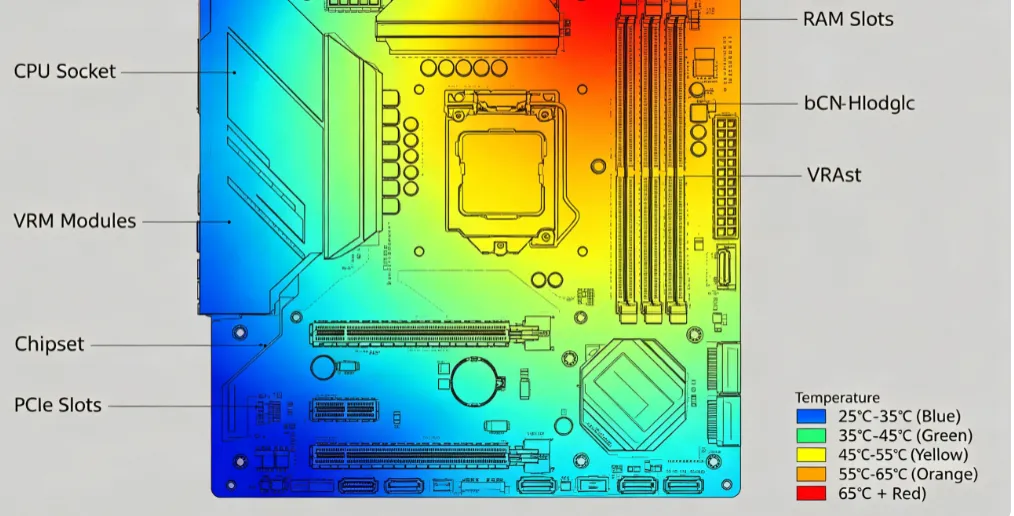
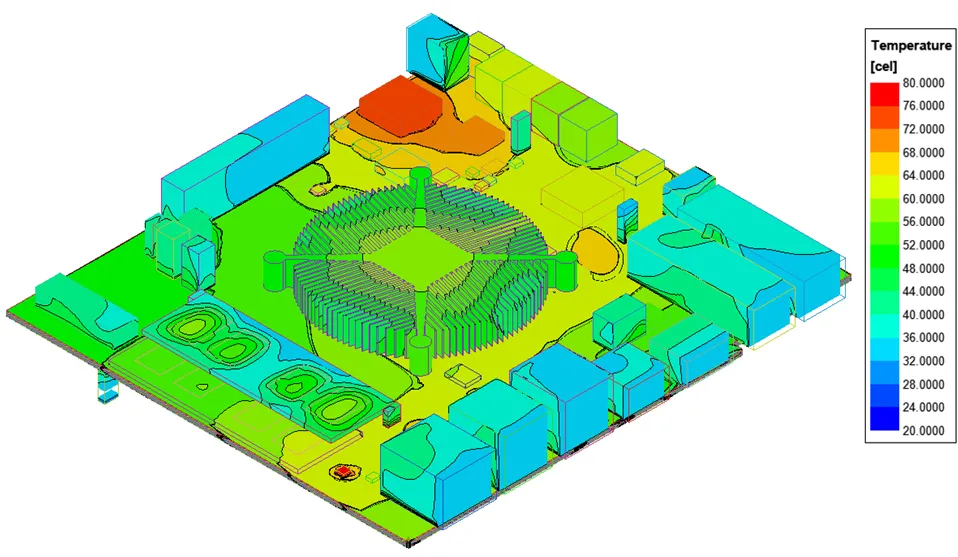
4. Thermal Management to Prevent Overheating
High-power grids generate significant heat, which can damage components or reduce efficiency. Effective thermal management in PCB design includes:
- Thermal Vias: Adding vias near heat-generating components to transfer heat to other layers or heat sinks, with a typical via density of 10-15 per square inch in high-power areas.
- Heat Sinks: Attaching heat sinks to critical components to dissipate heat, often reducing temperatures by 20-30°C.
- Component Placement: Spacing out high-power components to avoid concentrated heat buildup.
Thermal simulation tools can predict temperature rises and help optimize the design before manufacturing.
5. Minimizing Energy Loss with Optimized Layout
Energy loss in power distribution systems often occurs due to resistance, parasitic inductance, and poor layout. To achieve a PCB layout for minimal energy loss in distribution, consider:
- Short and Direct Traces: Reducing trace length minimizes resistance and inductance, cutting energy loss by up to 5-10% in high-current paths.
- Decoupling Capacitors: Placing capacitors near power pins to filter noise and stabilize voltage, with values typically ranging from 0.1 μF to 10 μF based on frequency needs.
- Balanced Current Distribution: Designing symmetrical layouts to ensure even current flow across the board.
These practices not only improve efficiency but also extend the lifespan of the PCB and connected components.
Challenges in Designing PCBs for Smart Grids
While designing PCBs that optimize power distribution systems offers many benefits, it comes with unique challenges:
- High Voltage and Current Stress: Components and traces must withstand voltages up to 600V or more and currents exceeding 20A in some grid applications.
- EMI and Noise: Smart grids rely on precise communication, and EMI can interfere with signals if not managed properly.
- Space Constraints: Equipment in smart grids often has limited space, requiring compact yet powerful PCB designs.
- Cost vs. Performance: Balancing the use of advanced materials and techniques with budget limitations can be tricky.
Addressing these challenges requires a combination of innovative design, simulation tools, and thorough testing.
Best Practices for Power Distribution Network PCB Solutions
To create effective power distribution network PCB solutions for smart grids, follow these best practices:
- Use Simulation Tools: Software for electrical and thermal simulation can identify potential issues like voltage drops or hotspots before production, saving time and cost.
- Adopt Multi-Layer Designs: Multi-layer PCBs with dedicated power and ground planes enhance stability and reduce noise, ideal for complex smart grid systems.
- Test Under Real Conditions: Prototype testing under actual grid conditions (e.g., varying loads and temperatures) ensures reliability in the field.
- Focus on Scalability: Design PCBs with future upgrades in mind, allowing for additional components or higher power capacities as smart grids evolve.
- Collaborate with Experts: Working with experienced PCB manufacturers ensures access to the latest materials and fabrication techniques tailored for high-power applications.
Future Trends in Power Distribution PCBs for Smart Grids
As smart grids continue to evolve, so do the technologies and designs for power distribution PCBs. Here are some trends to watch:
- Integration of IoT: PCBs will increasingly support IoT devices for real-time data collection and grid monitoring, requiring more complex signal routing.
- Advanced Materials: New substrates with even higher thermal conductivity and dielectric strength will become mainstream, supporting higher power densities.
- Miniaturization: Smaller, more efficient PCBs will be needed as smart grid equipment becomes more compact.
- Sustainability: Focus on eco-friendly materials and designs that reduce energy consumption aligns with the green goals of smart grids.
Staying ahead of these trends ensures that your PCB designs remain relevant and competitive in the fast-paced world of smart grid technology.
Conclusion: Building the Future of Smart Grids with Optimized PCBs
Power Distribution PCBs are indispensable in the development of smart grids, enabling efficient, reliable, and scalable power management. By focusing on power distribution in smart grids via PCBs, engineers can address the challenges of high-power systems through careful material selection, optimized layouts, and robust thermal management. Whether you're designing for minimal energy loss or seeking comprehensive power distribution network PCB solutions, the considerations and best practices outlined in this guide provide a solid foundation for success.
At ALLPCB, we’re committed to supporting engineers and designers with high-quality manufacturing and design services tailored to the unique needs of smart grid applications. With the right approach to PCB design for high-power grids and PCBs that optimize power distribution systems, you can contribute to a more efficient and sustainable energy future.